Nanotechnologists Discover How to Carve Tunnels Beneath the Surface of Silicon Chips
One of the enabling technologies of the modern world is the ability to construct ever smaller devices out of silicon. At first, these devices were purely electronic—diodes, transistors, capacitors and the like. But more recently, engineers have carved light pipes, fluid-pumping networks, and entire chemistry laboratories out of silicon.
The technique that makes all this possible is photolithography, which allows engineers to build on or etch the surface of silicon in very precise patterns. The devices—whether electronic, fluidic, or optical—are built up layer by layer. Everything is done in two dimensions on the surface of silicon and then added together to create 3-D shapes.
But what if it were possible to carve out structures beneath the surface of silicon, to create 3-D caves of almost any shape? Today, Onur Tokel at Bilkent University in Turkey and a few pals say they have developed just such a technique that can create networks of pipes and tunnels beneath the surface without any discernable change to the silicon surface.
The new technique relies on the fact that silicon is transparent to infrared light, which passes through silicon like sunlight through glass, at least at low intensities. When the light gets stronger, it can interact with electrons inside the material, generating currents and shaking the very crystal structure of the material. These effects are hard to predict and control but Tokel and co have found a way to use them to their advantage.
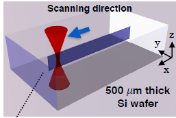
Their idea is simple in principle. They focus an infrared laser beam so that the focal point is deep inside a slab of silicon. At this point, the light intensity is so powerful that the photons begin to interact with the structure, dumping its energy inside the material.
The result is that the laser beam melts a tiny volume of silicon deep inside the structure creating a void. And by scanning the laser beam through the material, Tokel and co have created extended systems of tunnels of more or less any shape. By ensuring that the focal point always sits within the material, the silicon surface remains unchanged.
To show off the capabilities of the new technique, Tokel and co have created tunnels in the shape of grids, spirals, and even parallel sets of tunnels that act as barcodes. In other words, the technique can be used to store information.
That’s an interesting development. Tokel and co say the tunnels can easily be used as photonic channels to carry light or to carry liquids in microfluidic systems. They’ve even shown how they can store information that can be read by an ordinary smartphone camera that is sensitive to infrared light. “The demonstrated silicon processing technology can be used for the realization of multilayered silicon chips, optofluidics, and on-chip quantum optics experiments,” they say.
There are challenges ahead of course. One problem is that the team does not fully understand how the energy from the laser is transferred into the silicon. And without this knowledge, there is always a certain amount of guesswork involved in constructing these kinds of tunnels. “Detailed thermal simulations are required to further elucidate this phenomenon,” Tokel and co.
Nevertheless, the team has a powerful new technique on their hands that has the potential to change the way many types of silicon devices are built. Expect to hear a lot more about it.
Ref: arxiv.org/abs/1409.2827: Laser-Writing in Silicon for 3D Information Processing
Keep Reading
Most Popular
How scientists traced a mysterious covid case back to six toilets
When wastewater surveillance turns into a hunt for a single infected individual, the ethics get tricky.
The problem with plug-in hybrids? Their drivers.
Plug-in hybrids are often sold as a transition to EVs, but new data from Europe shows we’re still underestimating the emissions they produce.
What’s next for generative video
OpenAI's Sora has raised the bar for AI moviemaking. Here are four things to bear in mind as we wrap our heads around what's coming.
Stay connected
Get the latest updates from
MIT Technology Review
Discover special offers, top stories, upcoming events, and more.