The Next Big Thing at MIT Will Be Very, Very Small
Officially, it’s known as MIT.nano. But the people involved in the building’s construction like to call it “The Machine.”
It’s an apt name for the remarkable new facility taking shape within spitting distance of the Infinite Corridor. Designed to house two floors of clean-room space equipped with the world’s most advanced tools for nanoscale research, the building will indeed be a sort of high-tech machine, humming with air-handling equipment and hundreds of sensors constantly monitoring every aspect of the environment.
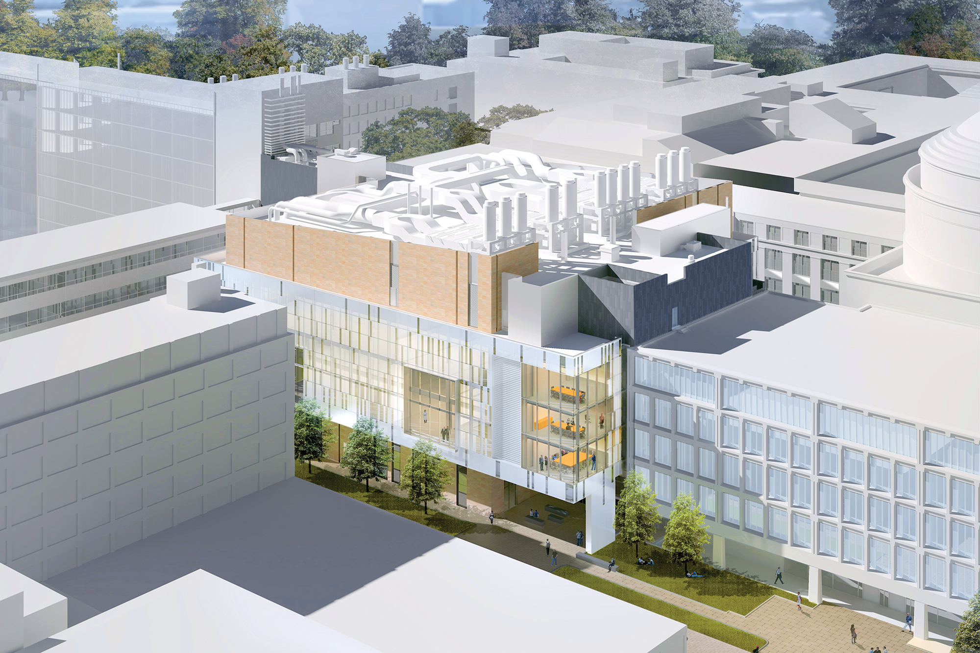
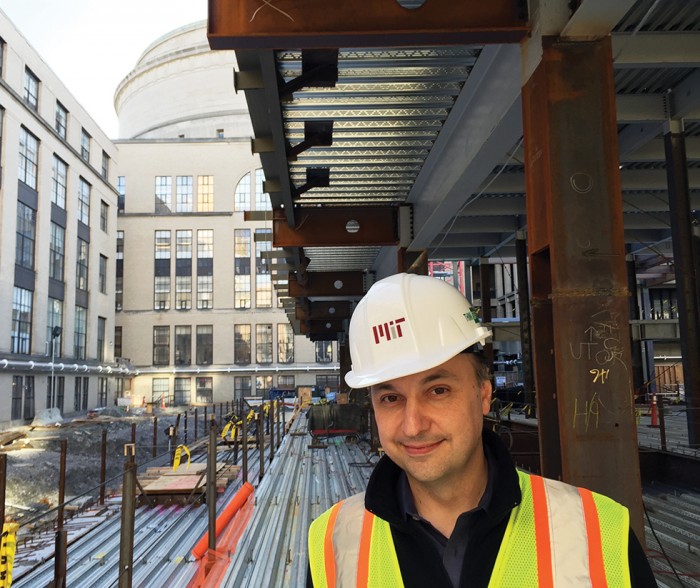
Anyone looking out the windows along the Infinite has seen a dramatic year of progress at the MIT.nano site, which is adjacent to MIT’s Building 10 with its Great Dome. What began as a very large hole in the ground has sprouted a steel frame with glass and concrete outer walls mostly in place. By the summer of 2018, research into structures at the scale of atoms and molecules will begin taking place inside the facility, whose construction is one of the largest, most ambitious, and most challenging building projects ever undertaken at MIT.

“Once completed, this will likely be the most complex building on the campus,” says Vladimir Bulović, MIT.nano’s faculty lead. “Its systems are highly integrated, and exquisitely tuned, as they would be in a complex, magnificent machine.”
Those systems will maintain the ultra-pristine environment that’s required to investigate nanotechnology. A few years from now someone walking by the glass-walled building may witness a researcher working on some new device that will revolutionize the manufacturing of pharmaceuticals, the purification of water, or the storage of electric power.
“The goal of MIT.nano is to contain every cutting-edge nanoscale tool that that could advance technology and science,” says Bulović, who is the Fariborz Maseeh Professor in Emerging Technology and associate dean for innovation in the School of Engineering. “It will allow you to manipulate anything from individual atoms to hand-held objects. It will provide a way to make [everything from] atomic-scale discoveries to micron-scale discoveries to millimeter-scale to hand-held size. We’ll be able to manipulate matter on a scale that you can’t do anywhere else on campus.”
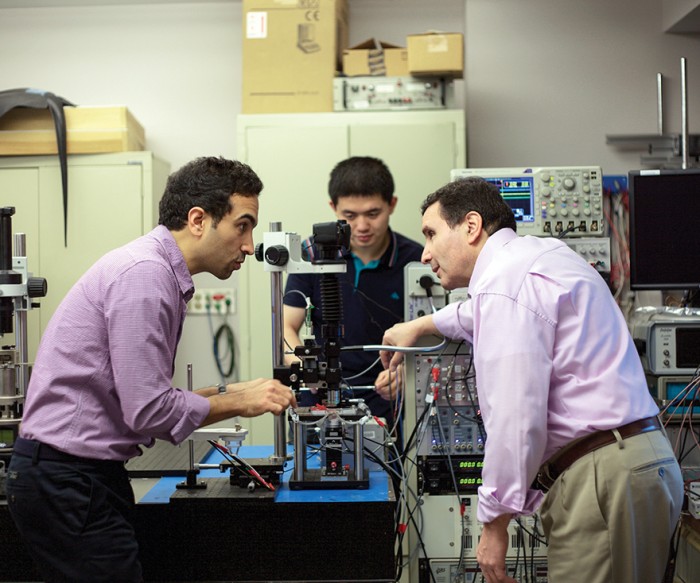
Today, researchers who need to use clean rooms and specialized tools for work on nanotechnology, which are housed on multiple floors of Building 39, must go to great lengths to avoid contaminating their samples—and must keep changing in and out of clean-room garb—as they carry their devices and work in progress from one such room to another. And demand for the necessary equipment is so high that some MIT researchers have had to do some of their work at Harvard.
MIT.nano will more than double the Institute’s shared space for nanoscale research, making centrally located, state-of-the art equipment easily accessible to everyone who needs it. “Think of it as an extreme maker space,” Bulović says.
Pushing atoms around
“We have known for many, many years that things matter down at the nanoscale,” says Bulović. But for a long time, “we didn’t have a chance to really take a look.” Then, in 1981, researchers at IBM invented the scanning tunneling microscope, the first tool that could “see” individual atoms. And that, he says, “brought us closer to an appreciation of why the nanoscale does what it does.”
“Many of the things we experience or use in daily life are based on nanotechnology, but we don’t really appreciate that,” Bulović says. “The detergents provide the brighter-than-white glow of clean clothes because they use nanoscale phosphors. Everything you smell is molecules of scent that happen to be one nanometer in size—your nose has nanoscale detectors in order to sense that smell. Our taste buds sense nanoscale and microscale features in our food—that’s what gives us the sensation of taste. Why does the ceramic tile feel colder than the wooden floor, when in fact they are both the same temperature? It’s the atomic-scale, nanoscale attachment of the atoms and the way they conduct heat away from your body that is different.”
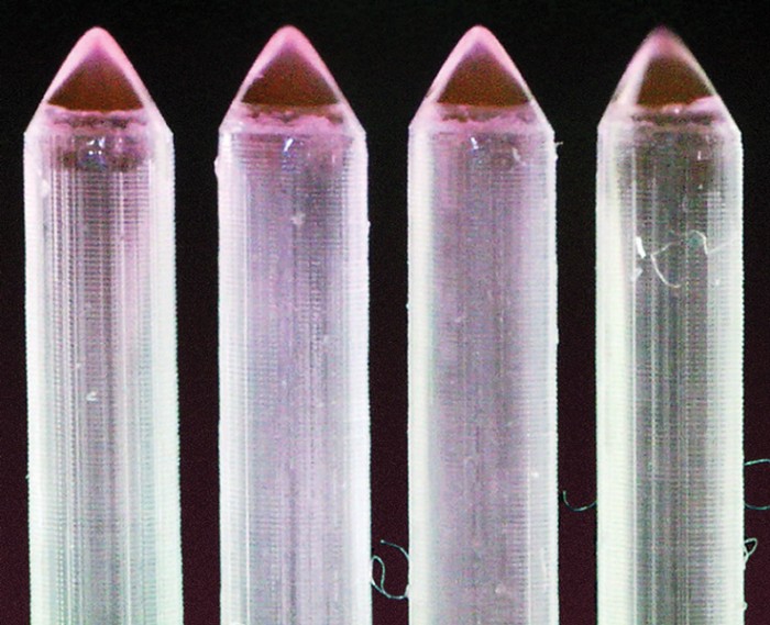
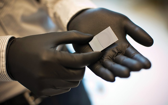
Since gaining the ability to look at atoms, researchers have increasingly learned how to manipulate and create structures on that scale. Now nanotechnology—making or manipulating materials in which at least one of the three dimensions is measured in nanometers (billionths of a meter)—is at the forefront of a staggering range of work. It’s being used to develop new kinds of systems for pharmaceutical manufacturing and drug delivery, radically new materials for capturing solar energy, highly efficient ways of purifying water, biocompatible fibers that could deliver both stimuli and medications while returning data on the body’s responses, robotic devices capable of manipulating molecules, structured nanomaterials that may unleash the power of quantum computation, and much more.
Nanotechnology, by its nature, is multidisciplinary. Indeed, the kinds of research that will be carried out in the clean rooms, imaging facilities, and prototype fabrication spaces at MIT.nano could have profound impacts across a swath of scientific and engineering fields so broad that an estimated 2,000 faculty members, postdocs, and students are expected to use the facility annually. Among newly tenured faculty, more than half in the School of Science, and two-thirds in the School of Engineering, will probably take advantage of it.
Giving researchers that access could yield big results. For example, Bulović says, the world now runs mostly on electricity, but its production and use can be highly inefficient—and nanotechnology could bring improvements in many areas, including photovoltaics. “There are some options coming forward that could redefine the way solar cells perform, because you can start using the nanoscale structure of materials, or quantum dots, to generate solar cells that are thinner, lighter, more deployable than any previous solar technology, and as a result more scalable,” he says. “That would be a game changer.”
Nanotechnology could also help avert a looming crisis in energy use for computing. Cloud computing today consumes “maybe 3 or 4 percent” of the electricity used across the globe, Bulović says, but that’s growing fast: “There is a projection that we’ll need a thousandfold more cloud computing a decade from now.” With new chips based on nanotechnology, huge leaps in efficiency might avoid the resulting power crunch.
New opportunities in nano sensing hold great promise as well. Researchers including Timothy Swager are working on a multifunction electronic nose that could sense explosive traces in the air, chemicals present on surfaces, or gases that indicate when produce is ripe.
And a similar approach could transform health care. “If you can monitor gases coming out in your breath, would you be able to infer the health state of an individual? You could—you just need the right kind of chemical sensor,” Bulović says.
“The way we want to affect those cells, control them, improve them, cure them, deliver medicines: nanoscale medicine is a tremendous frontier. It’s the functional scale of the operation of our bodies.”
Building a ship in a bottle
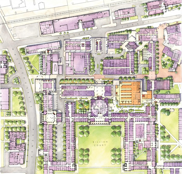
Constructing the MIT.nano building represents a daunting engineering challenge. The building’s site was chosen because it’s subject to far less vibration from traffic, subways, and trains, and far less electromagnetic interference, than any of the other four potential locations. Even barely perceptible disturbances of that nature could wreck an experiment or distort an image at the nanoscale. But the location is at the very heart of campus. That made getting truckloads of materials in or out so tight a squeeze that the team responsible for the project likens it to building a ship in a bottle.
One of countless tricky tasks was pouring the concrete base for the building’s imaging devices on the basement level. “There’s a four-million-pound slab that’s in the basement, on which the most sensitive of the instruments will sit,” Bulović explains. “That slab needed to be poured in a single one-day pour. How do you deliver four million pounds of concrete to a site, when you only have 90 minutes from when concrete is batched until it’s poured—and it hardens 15 to 30 minutes after delivery? You have to make sure you have exactly the right timing. To deliver that much you need 90 cement trucks, and they all need to be coördinated to arrive just at the right moment. It took about eight hours of perfect coördination. I refer to it as the cement truck ballet.”
Meanwhile, three narrow openings between and under buildings provided the site’s only access for trucks and heavy equipment including cranes, says Travis Wanat, the project’s construction manager. To assemble the many pieces of two tower cranes, which have been essential in extracting thousands of tons of dirt and gently lowering in hundreds of tons of steel beams and other materials, “we needed a mobile crane, and that was really, really tight getting that into the site,” Wanat recalls. To allow the truck carrying the mobile crane to inch under the bridge between Buildings 35 and 37, he says, “at one point we had to let a certain amount of air out of
the tires.”
And the complications are far from over. “The next most challenging delivery is going to be the air-handling units and exhaust units,” Wanat says. “We built a life-size replica of the largest piece of each unit out of PVC pipe, and put it on the back of a truck and drove it through the pathway that we would take, to make sure we have the right clearances. Better to do it with plastic pipe than with a metal box!”
Much of the interior of this building will be about 10,000 times cleaner than ordinary room air—achieving what’s known as level 5 cleanliness, meaning there are fewer than 100 particles larger than half a micrometer in every cubic foot of space. By comparison, indoor air typically has a million such particles per cubic foot.
That extreme cleanliness is essential, because at the scale of the nanoparticles, nanofilms, and nanofibers that researchers will be studying, one particle of dust could ruin a whole experiment. Achieving it begins during the construction process. Workers building the clean rooms will have to follow strict protocols as they enter the worksite. “It’s treated like it was a research clean room, where there’s training for everyone who has to go in that room,” says Wanat. “Depending on what level [of cleanliness] we’re at, they’ll need to wear the Tyvek suits, the booties, the gloves, the hair nets, as we progress through the stages of that project.”
A new crossroads for the campus
Because nanotechnology is at the intersection of biology, chemistry, electronics, physics, and engineering (among many other disciplines), it was a fortuitous coincidence that the quietest location on campus in terms of vibration turned out to be close to the center of campus as well. So the team planning the building aimed to create a space that will encourage collaboration and serendipity.
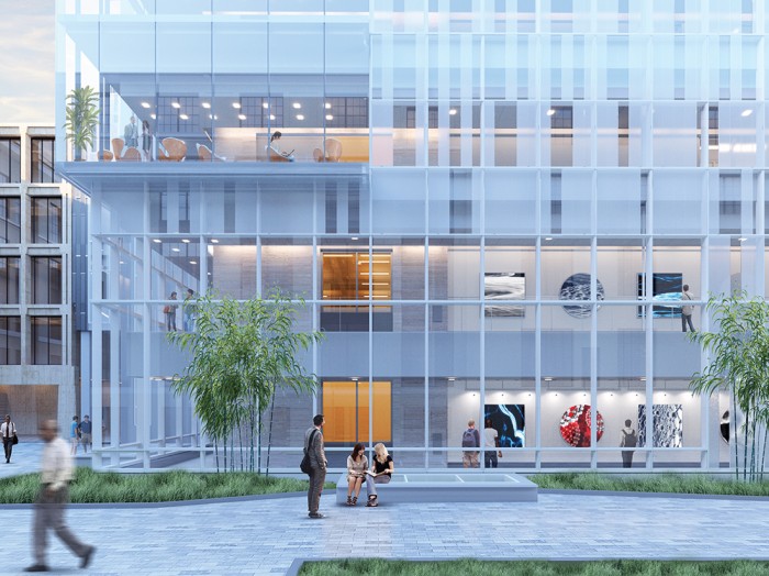
Bulović says that despite its many barriers against outside dust and vibration, the space will be very open. “It needs to be a contained environment, but why not put windows everywhere, so that you can look inside and see what’s happening in there?” he says.
Indeed, the building will be remarkably porous visually, in places allowing light to shine all the way through from one side and out the other. Its exterior walls, which will be completed this fall, are largely made of glass, as are many of the interior walls of the labs and clean-room space. Visitors will be able to walk along wide corridors on each level that will have views of the courtyard and buildings outside, including the Great Dome—and they’ll be able to watch researchers in full protective coveralls, hoods, goggles, and booties as they carry out their experiments.
“Within the clean room itself, we wanted to have visual communication from one end to the other,” Bulović says. “So we have long corridors that are optically unimpeded. The walls and bays and chases are transparent. You can look in and see the machinery, and the person in the next bay and the next bay.”
He envisions MIT.nano as a place that facilitates accidental encounters, rather than just a place where people come to use the tools as they would in a typical machine shop. “It has to be a place that allows you to spark a conversation, allows you to have a place to step aside from the tool and go to a whiteboard—or a magnetic board, because we don’t want dust—and sketch out the next idea,” he says. “We have common areas that provide for those chance encounters.”
Once the facility opens in June of 2018, filling all of its space with fabrication and imaging tools could take another two to three years, Bulović says, though basic kinds of equipment should be available much earlier. And that delay is by design: to ensure that MIT.nano will give researchers access to tools that are truly state-of-the-art in a field that is advancing rapidly, the final choices of equipment won’t be made until the new building is ready—and until the funding is in place for those devices. Ultimately, the labs are expected to house a panoply of devices that will allow not only nanoscale imaging, vacuum deposition, and biological analysis, but also such activities as fabricating and assembling nano devices, designing and testing chips, and making two-dimensional materials and nanofibers. Some of these devices don’t even exist yet. Potential users of the facility are already invited to suggest tools they’d like to have available; initial selections based on community input will begin next year.
Meanwhile, the outer walls are rapidly taking their final form. And with that shell soon to be fully in place, the construction of MIT.nano will no longer be quite as much of a spectator sport as the process has been for the last two years. But it won’t be totally out of view, Wanat says: “We’re looking to set up time-lapse cameras in the corners. So hopefully once we get the exterior walls up, there will still be some views inside the building that we can project to the community as we go along.”
Keep Reading
Most Popular
Large language models can do jaw-dropping things. But nobody knows exactly why.
And that's a problem. Figuring it out is one of the biggest scientific puzzles of our time and a crucial step towards controlling more powerful future models.
How scientists traced a mysterious covid case back to six toilets
When wastewater surveillance turns into a hunt for a single infected individual, the ethics get tricky.
The problem with plug-in hybrids? Their drivers.
Plug-in hybrids are often sold as a transition to EVs, but new data from Europe shows we’re still underestimating the emissions they produce.
Stay connected
Get the latest updates from
MIT Technology Review
Discover special offers, top stories, upcoming events, and more.