Diamond Patterning Technique Could Transform Photonics
One of the enabling technologies of our time is photolithography, the process that creates patterns on the surface of materials such as silicon, silicon dioxide and other components of microelectronic devices.
It’s hard to overstate the importance of this technique. Almost all microchips are made using it so the fruits of this invention permeate our world.
Now computer scientists have begun to look beyond silicon for the next generation of chips and the ones beyond that. And one of the most exciting materials they are investigating is diamond.
But there is a problem. Making devices out of diamond is a difficult business because of its chemical robustness. Photolithography simply does not work.
Instead, physicists can only carve the surface of diamond using high-energy processes such as high-power laser ablation and ion bombardment. And these often destroy the surface and anything on it.
What they need insread is a process that produces patterns on the surface of diamond as easily as photolithography does with silicon.
Today, Aiden Martin and buddies at the University of Technology in Sydney, Australia, say they developed such a technique. They’ve found a way of fabricating structures out of diamond using a low-energy technique that does not damage the surface or destroy structures nearby.
The new technique is relatively straightforward. It relies on the fact that water molecules tend to adhere to the surface of diamond. Martin and co then break apart the water molecules with low energy electrons creating hydrogen and oxygen radicals. The oxygen radicals are so reactive that they rip carbon molecules out of the diamond crystal forming carbon monoxide.
The result is a low energy process that removes carbon atoms relatively gently. Creating a pattern on the surface of diamond is then simply a question of finding a way to prevent water molecules adhering to the diamond surface or of blocking the action of electrons in a predefined shape.
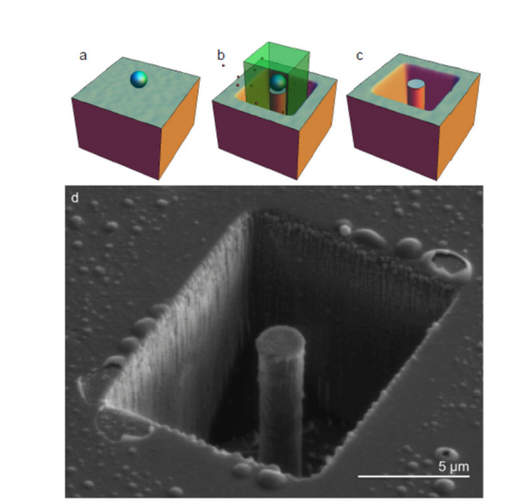
Martin and co demonstrate their technique using a mask of silica placed on a diamond surface, which bars the passage of low energy electrons. They then place the diamond in an atmosphere of water vapour and then scan a low energy electron beam over the exposed surface to remove the diamond.
The results are impressive. The team has created diamond pillars, has carved patterns into diamond surfaces and has even written words on nanodiamond facets at an angle to the electron beam.
That has many potential applications. “The electron induced chemical etching paves the way to a transformative technology for nanofabrication of diamond,” say Martin and co.
One of the most exciting possibilities is in quantum computing, where the ability to manipulate single photons is crucial. That’s possible with diamond thanks to a phenomena called nitrogen vacancy luminescence, in which a nitrogen atom is substituted into the diamond structure instead of a carbon.
Since nitrogen has one less electron in its outer shell, it creates a vacancy in the crystal. And this can be used for everything from producing photons to detecting magnetic or electric fields, all at room temperature.
With the new technique it suddenly becomes possible to fabricate all kinds of structures with nitrogen vacancy centres in them. “It is the first step towards rendering 3D single crystal diamond geometries for high performance photonic, sensing and quantum devices,” say Martin and co.
The team calls its new technique electron beam induced etching or EBIE. Expect to hear a lot more about it.
Ref: arxiv.org/abs/1403.4067 : Subtractive 3D Printing of Optically Active Diamond Structures
Keep Reading
Most Popular
Large language models can do jaw-dropping things. But nobody knows exactly why.
And that's a problem. Figuring it out is one of the biggest scientific puzzles of our time and a crucial step towards controlling more powerful future models.
How scientists traced a mysterious covid case back to six toilets
When wastewater surveillance turns into a hunt for a single infected individual, the ethics get tricky.
The problem with plug-in hybrids? Their drivers.
Plug-in hybrids are often sold as a transition to EVs, but new data from Europe shows we’re still underestimating the emissions they produce.
Stay connected
Get the latest updates from
MIT Technology Review
Discover special offers, top stories, upcoming events, and more.