The chip patterning machines that will shape computing’s next act
The first lithography tools were fairly simple, but the technologies that produce today’s chips are among humankind’s most complex inventions.
When we talk about computing these days, we tend to talk about software and the engineers who write it. But we wouldn’t be anywhere without the hardware and the physical sciences that have enabled it to be created—disciplines like optics, materials science, and mechanical engineering. It’s thanks to advances in these areas that we can fabricate the chips on which all the 1s and 0s of the digital world reside. Without them, modern computing would have been impossible.
Semiconductor lithography, the manufacturing process responsible for producing computer chips, has 70-year-old roots. Its origin story is as simple as today’s process is complex: the technology got its start in the mid-1950s, when a physicist named Jay Lathrop turned the lens in his microscope upside down.
Lathrop, who died last year at age 95, is scarcely remembered today. But the lithography process he and his lab partner patented in 1957 transformed the world. Steady improvement in lithographic methods has produced ever-smaller circuitry and previously unimaginable quantities of computing power, transforming entire industries and our daily lives.
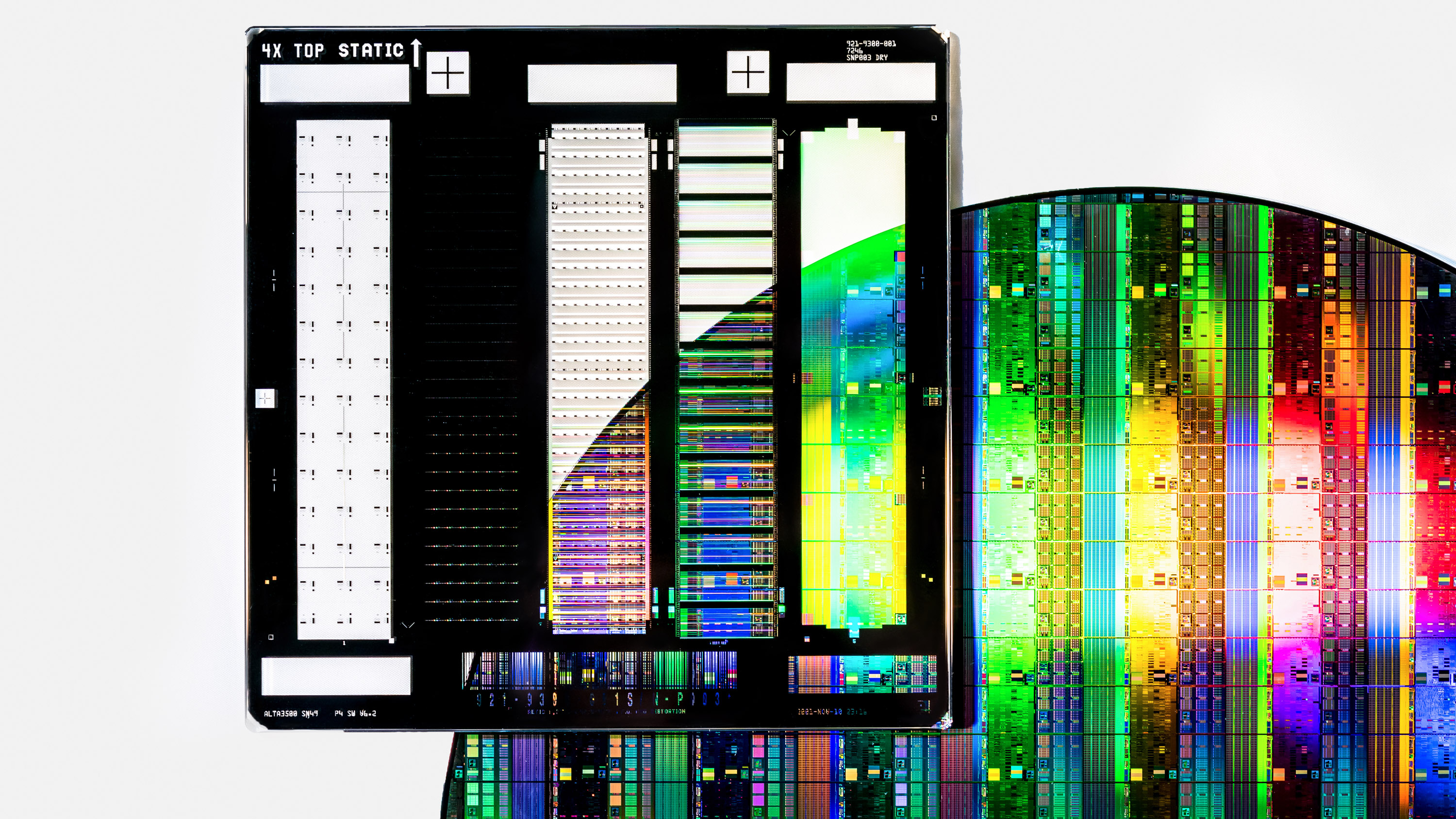
Today lithography is a big business with tiny margins for error. The world leader, the Dutch firm ASML, is also Europe’s largest tech company by market capitalization. Its lithography tools—which rely on the world’s flattest mirrors, one of the most powerful commercial lasers, and an explosion far hotter than the surface of the sun—can pattern tiny shapes on silicon, measuring just a handful of nanometers. This nanometer-scale precision, in turn, makes it possible to manufacture chips with tens of billions of transistors. You probably rely on chips made with these ultra-advanced lithography tools; they can be found in your phone, your PC, and the data centers that process and remember your data.
Of all the mind-bogglingly precise machines that manufacture chips, lithography tools are the most critical—and the most complex. They require hundreds of thousands of components and billions of dollars of investment. But they are not only the subject of commercial rivalry and scientific wonder; they stand at the center of a geopolitical competition to control the future of computing power. Where computing goes next will be shaped by the evolution of the lithography industry—and the struggle to produce even more precise lithography tools. The history of the technology’s development suggests that any future advances will rely on even more complex and precise machinery, and even more far-flung supply chains, to produce the specialized components required. The speed at which new lithography systems and components are developed—and the question of which companies and countries manage to manufacture them—will shape not only the speed of computing progress but also the balance of power and profits within the tech industry.
The idea that today’s nanometer-scale manufacturing has its origins in Lathrop’s upside-down microscope lens might seem implausible. But the lithography industry has advanced rapidly. It has enabled chips to follow—and set the pace of—Moore’s Law, the idea that the number of transistors in an integrated circuit doubles roughly every two years.
Lathrop invented the process in the 1950s, at a time when computers used vacuum tubes or transistors so large they were visible to the naked eye—and thus easy enough to manufacture without having to create an entirely new class of tools.
He wasn’t trying to revolutionize computing; he later recalled that he had “no idea about computers.” As an engineer at the US Army’s Diamond Ordnance Fuze Lab during the mid-1950s, he’d been tasked with devising a new proximity fuze to go inside a mortar shell only a couple of inches in diameter. One of the components his fuze required was a transistor—but the shell was so small that existing transistors were difficult to fit inside.
At the time, transistor manufacturing was in its early stages. Transistors were used as amplifiers in radios, while discrete transistors were beginning to be used in computers the size of rooms. The fuze lab already had some equipment for making transistors, such as crystal growers and diffusion furnaces. But even at an advanced weapons lab, many of the materials and tools needed to fabricate them had to be developed from scratch.
These early transistors were made of a block of the chemical element germanium with different materials layered on top, so they resembled the shape of a desert mesa. These flat-topped blocks of material were made by first covering a portion of the germanium with a drop of wax. A chemical was then applied, which etched away the germanium that wasn’t covered. When the wax was removed, only the germanium that it covered was left behind, sitting on a metallic plate. This system worked well enough for large transistors, but miniaturizing them was all but impossible. The wax oozed in unpredictable ways, limiting the precision with which the germanium could be etched. Lathrop and his lab partner, Jim Nall, found their progress on the proximity fuze stuck in the imperfections of overflowing wax.
Lathrop had spent years looking through microscopes to make something small look bigger. As he puzzled over how to miniaturize transistors, he and Nall wondered whether microscope optics turned upside down could let something big—a pattern for a transistor—be miniaturized. To find out, they covered a piece of germanium material with a type of chemical called a photoresist, which they acquired from Eastman Kodak, the camera company. Light reacts with photoresist, making it either harder or weaker. Lathrop took advantage of this feature and created a “mask” in the shape of a mesa, placing it on the microscope with upside-down optics. Light that passed through holes in the mask was shrunk by the microscope’s lens and projected onto the photoresist chemicals. Where the light struck, the chemicals hardened. Where light was blocked by the mask, they could be washed away, leaving a precise, miniature mesa of germanium. A way to manufacture miniaturized transistors had been found.
Lathrop named the process photolithography—printing with light—and he and Nall filed for a patent. They delivered a paper on the topic at the annual International Electron Devices Meeting in 1957, and the Army awarded him a $25,000 prize for the invention. Lathrop bought his family a new station wagon with the money.
In the midst of the Cold War, the market for mortar fuzes was growing, but Lathrop’s lithography process took off because companies producing transistors for civilian electronics realized its transformative potential. Lithography not only produced transistors with unprecedented precision but also opened the door to further miniaturization. The two companies leading the race to commercial transistors—Fairchild Semiconductor and Texas Instruments—understood the implications early on. Lithography was the tool they needed to manufacture transistors by the millions, turning them into a mass-market good.
Painting with light
Robert Noyce, one of the cofounders of Fairchild, had studied alongside Lathrop when both had been PhD students in physics at MIT. The two of them had spent their weekends in graduate school hiking New Hampshire’s mountains, and they had stayed in touch after graduating. At Fairchild, Noyce moved quickly to hire Nall, Lathrop’s lab partner, and spearheaded his company’s lithography efforts by jury-rigging his own device with a set of 20-millimeter camera lenses he’d bought from a Bay Area photography shop.
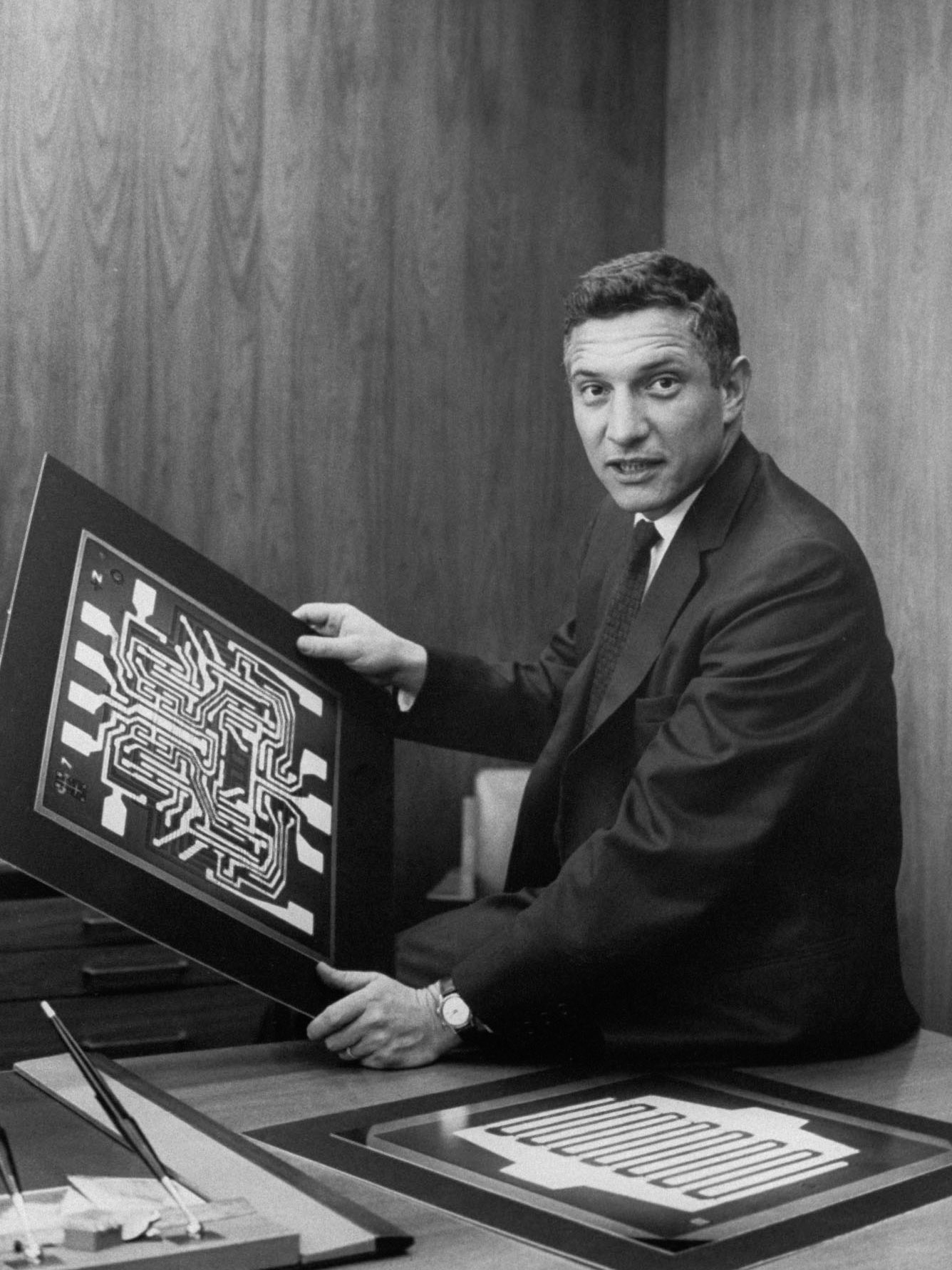
Lathrop, meanwhile, took a job at Fairchild’s competitor, Texas Instruments, driving his new station wagon down to Dallas. He arrived just as his new colleague and lifelong friend Jack Kilby was on the brink of creating a piece of semiconductor material with multiple electronic components built—or integrated—into it. These integrated circuits, it soon became clear, could be efficiently produced only with Lathrop’s lithography method. As chip firms strove to shrink transistors to cram more of them onto chips, photolithography provided the precision that miniaturized manufacturing required.
Fairchild and Texas Instruments made their first lithography machines in house, but the growing complexity of the machines soon attracted new entrants. As the scale of transistors declined from centimeters to millimeters to microns, the importance of precision optics increased. Perkin-Elmer was a Connecticut-based firm that produced specialized optics for the US military, from bombsights to spy satellites. In the late 1960s, it realized that this expertise could be used for lithography, too. It developed a scanner that could project the mask pattern onto a silicon wafer while aligning them with almost flawless precision. The scanner then moved a light across the wafer like a copy machine, painting it with lines of light. This tool proved capable of fabricating transistors as small as a micron—one millionth of a meter.
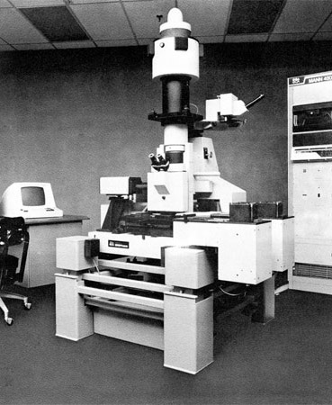
But the approach wasn’t practical as chip features got still smaller. By the late 1970s, scanners began to be replaced with steppers, machines that moved light in discrete steps across a wafer. The challenge with a stepper was to move the light with micron-scale precision, so that each flash was perfectly aligned with the chip. GCA, a Boston-based firm that had its origins in spy balloons, devised the first stepper tool, reportedly on the advice of Texas Instruments executive Morris Chang—later the founder of TSMC, which is today the world’s largest chipmaker.
New England’s specialist lithography firms soon faced steep competition. In the 1980s, as Japanese chipmakers began winning major market share in the production of memory chips, they started buying from Nikon and Canon, two homegrown producers of lithography tools. Around the same time, the Dutch chipmaker Philips spun out its own unit that made lithography tools, calling the new company ASML.
GCA, which remained America’s lithography champion, struggled to cope with the competition. Its lithography technology was widely recognized as top-notch, but the machines themselves were less reliable than those from its new Japanese and Dutch rivals. Moreover, GCA failed to anticipate a series of chip industry business cycles in the 1980s. It soon found itself financially overextended and, by the end of the decade, on the brink of bankruptcy. Bob Noyce tried to rescue the firm; as the head of Sematech, a government-backed semiconductor research institute intended to revitalize the US chip industry, he poured millions of dollars into GCA. Yet it wasn’t enough to stop the firm from hurtling toward collapse. The lithography industry thus entered the 1990s defined by three firms, two Japanese and one Dutch.
The decline of an industry
The decline of America’s lithography industry coincided with a dramatic leap forward in the field’s technological complexity. Visible light—which has a wavelength of several hundred nanometers—was by the 1980s too broad a brush with which to paint the smallest transistors. So the industry shifted to using new chemicals like krypton fluoride and argon fluoride to create deep ultraviolet light, with wavelengths as low as 193 nanometers. By the early 2000s, after this ultraviolet light itself proved too blunt a tool, lithography machines were created that could shoot light through water, creating a sharper angle of refraction and thereby allowing more precision. Then, after this “immersion” lithography proved insufficient for the finest features on a chip, lithographers began using multi-patterning, applying multiple layers of lithography on top of one another to produce yet more precise patterns on silicon.
As early as the 1990s, however, it was clear that a new light source with a smaller wavelength would be needed to continue manufacturing ever-smaller transistors. Intel, America’s biggest chipmaker, led the early investments into extreme ultraviolet (EUV) lithography, using a type of light with a wavelength of 13.5 nanometers. This was sufficiently exact to pattern shapes with roughly equivalent dimensions. But only one of the world’s remaining lithography companies, ASML, had the guts to bet its future on the technology, which would take three decades and billions of dollars to develop. For a long time, many industry experts thought it would never work.
Producing EUV light at sufficient scale is one of the most complex engineering challenges in human history. ASML’s approach requires taking a ball of tin 30 microns wide and pulverizing it twice with an ultra-high-powered carbon dioxide laser. This explodes the tin ball into a plasma with a temperature of several hundred thousand degrees. The plasma emits EUV light, which then must be collected with the flattest mirrors ever created, each made of dozens of alternating, nanometers-thick layers of silicon and molybdenum. These mirrors are held almost perfectly still by a set of actuators and sensors that, their manufacturer says, are so precise they could be used to direct a laser to hit a golf ball as far away as the moon.
Producing the specialized components in an EUV system required constructing a complex international supply chain. The high-powered laser is manufactured by a German firm called Trumpf, which specializes in precision cutting tools. The mirrors are produced by Zeiss, another German firm with a proud history of expertise in optics. The chamber in which the tin balls are pulverized was designed by Cymer, a San Diego firm later purchased outright by ASML. A machine with hundreds of thousands of components can be produced only with participation from companies on multiple continents, even if its assembly is monopolized by a single firm.
Today, EUV lithography tools are used to produce many of the key chips in phones, PCs, and data centers. A typical smartphone processor will have over 10 billion microscopic transistors, each printed by the photolithography process Lathrop pioneered. Lithography has been used to create transistors by the quintillions, making them the most widely produced manufactured product in human history.
Perhaps most important, however, is the role of EUV lithography in producing the chips that advanced data centers require. Large AI systems are usually trained on cutting-edge chips—which means they benefit from the ultra-advanced transistors that only EUV lithography can fabricate efficiently. This has made lithography a matter of geopolitical jostling. As the US tries to stop China’s chip industry from producing cutting-edge AI chips, it has limited Beijing’s access to critical tools. EUV lithography systems are the biggest choke point for China’s chip industry.
The fact that the computing capabilities of the world’s second-largest economy depend on access to a single tool produced by a single company illustrates the central role lithography plays in the world’s tech sector. The industry is extraordinarily complex—the result of intensive research efforts by a worldwide network of experts on optics and materials science, plus billions of dollars of investment. China’s homegrown lithography tools are several generations behind the cutting edge, lacking many of the key components—like the ultra-flat mirrors—as well as the expertise in systems integration.
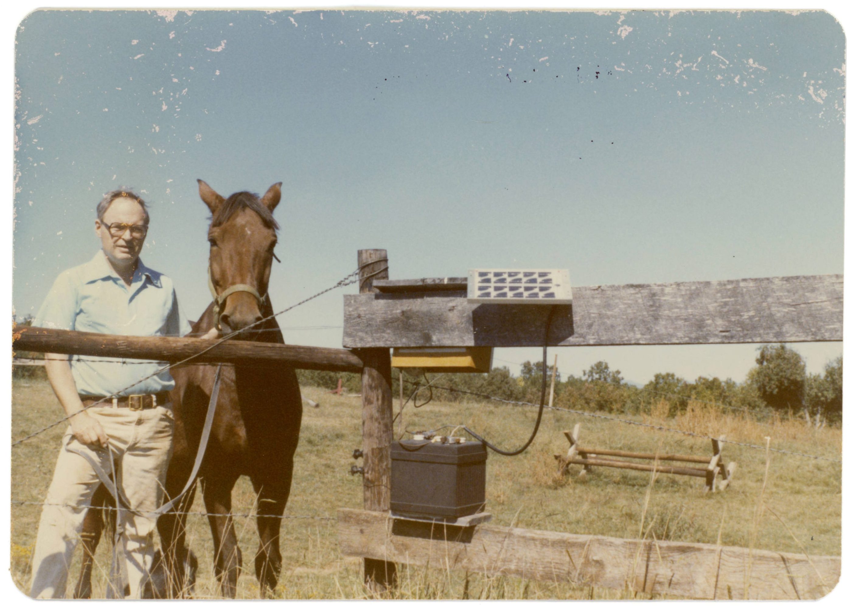
The industry has come a long way since Lathrop’s work on fuzes. He left Texas Instruments in 1968, having worked there for a decade, and took up a professorship at Clemson University, where his father had studied and not far from where his parents then lived. Lathrop spent the rest of his career teaching, though in the summers during the 1970s and 1980s he would return to TI to work with his old friend Jack Kilby on an unsuccessful effort to develop photovoltaic technology for solar power. Lathrop retired from Clemson in 1988, having left an imprint on thousands of electrical engineering students.
The lithography process he invented, meanwhile, continues to advance. In several years, ASML will release a new version of its EUV technology, called high-numerical-aperture EUV, which will allow even more precise lithography. Research into a future tool with even more precision is underway, though it is unclear if it will ever be practically or commercially feasible. We must hope it is, because the future of Moore’s Law—and the advances in computing it enables—depend on it.
Chris Miller is author of Chip War: The Fight for the World's Most Critical Technology and an associate professor at the Fletcher School at Tufts University.
Deep Dive
Computing
How ASML took over the chipmaking chessboard
MIT Technology Review sat down with outgoing CTO Martin van den Brink to talk about the company’s rise to dominance and the life and death of Moore’s Law.
Why it’s so hard for China’s chip industry to become self-sufficient
Chip companies from the US and China are developing new materials to reduce reliance on a Japanese monopoly. It won’t be easy.
Stay connected
Get the latest updates from
MIT Technology Review
Discover special offers, top stories, upcoming events, and more.