A Tough Tip for Nano Manipulation
IBM’s Zurich Research Laboratory—where several groundbreaking microscopy tools have been invented—has created a tough new coating for the tip of an atomic force microscope (AFM), a device that can be used to capture nanoscale imagery as the tip is run over a surface on the end of a microscopic cantilever. The coating could expand the range of ways that AFM can be used to include making lithographic masks for electronic manufacturing with features 10 nanometers in size—beyond the limits of traditional processes such as e-beam lithography.
Scientists have long wanted to use atomic tips in such ways, but it’s difficult to prevent the silicon tips from wearing down too quickly as they move across a surface, says Mark Lantz, manager of storage research at IBM’s Zurich Research Laboratory.
A common way to make atomic tips more wear-resistant is to add a diamond coating. But diamond is surprisingly unstable, says Lantz. It will burn when heated to around 400 °C, which is impractical for certain uses. IBM had originally set its sights on using heated arrays of tips to burn pits in thin polymer substrates as a way of storing digital memory—a concept known as millipede memory. IBM is no longer pursuing millipede memory as a consumer technology, although it hopes to adapt it for archival storage systems or high-speed biological imaging of subcellular processes.
The IBM researchers apply a layer of silicon carbide, a material that is slightly softer than diamond but does not burn when heated. “Silicon carbide has an extremely high melting temperature, so even at 1,400 °C, it still maintains its strength,” says Lantz.
The team came up with a novel process to create the silicon carbide coating. It was developed in collaboration with Robert Carpick and colleagues at the University of Pennsylvania and Kumar Sridharan and colleagues at the University of Wisconsin. Details of the work were published yesterday in the journal Advanced Functional Materials.
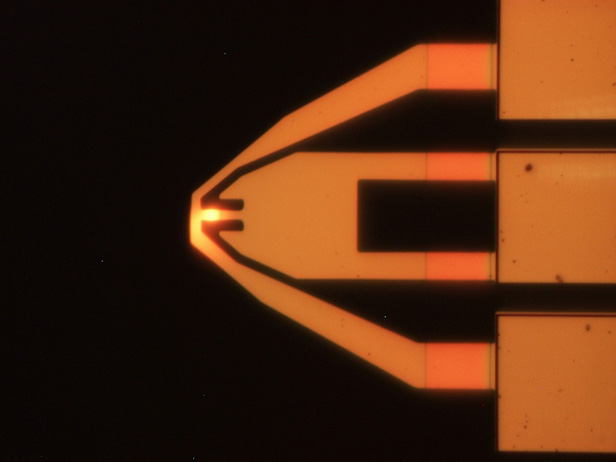
The process involves implanting carbon ions in a tip by surrounding the tip with plasma containing the carbon ions, then applying a high voltage between the plasma and the tip, causing the ions to become embedded in its surface. Next, the tip is heated to 1,100 °C, a temperature sufficient to make the carbon ions react with nearby silicon atoms to form a thin coating of silicon carbide. “The coating thickness is about 15 to 18 nanometers, and at the very apex of the tip, where the dimensions become less than this, the last 30 nanometers of the tip, is just pure silicon carbide,” says Lantz.
Chad Mirkin, director of the International Institute for Nanotechnology, at Northwestern University, says that in general, and for tasks such as memory storage, “the biggest issue that limits utility is speed.” But he adds that using an AFM to make a lithographic mask would make sense, since speed is not as important.
Keep Reading
Most Popular
Large language models can do jaw-dropping things. But nobody knows exactly why.
And that's a problem. Figuring it out is one of the biggest scientific puzzles of our time and a crucial step towards controlling more powerful future models.
How scientists traced a mysterious covid case back to six toilets
When wastewater surveillance turns into a hunt for a single infected individual, the ethics get tricky.
The problem with plug-in hybrids? Their drivers.
Plug-in hybrids are often sold as a transition to EVs, but new data from Europe shows we’re still underestimating the emissions they produce.
Stay connected
Get the latest updates from
MIT Technology Review
Discover special offers, top stories, upcoming events, and more.