A new way to make ultrathin ribbons of graphene could give the promising electronic material the edge it needs to finally become practical for use in digital processing on computer chips. Researchers have shown that they can grow the nanoribbons, a geometry that is crucial if the material is to made into high-performing transistors, directly on a wafer like those used in the semiconductor industry.
High-quality graphene nanoribbons can now be grown directly on a conventional germanium wafer.
The electronic and thermal properties of graphene, a single-atom-thick layer of carbon, are tantalizing to technologists who see it as the potential basis for new kinds of computer chips that are faster, use less power, and can flex and bend. But graphene on its own does not have the characteristics necessary for transistors that are energy-efficient enough to be practical. That’s because it is not a semiconductor. It does not have a band gap, the electronic property that is necessary for switching transistors between two discrete states—one in which electrons flow freely and one in which they don’t.
Advertisement
In recent years, however, researchers have shown that graphene ribbons narrower than 10 nanometers do act like semiconductors, exhibiting a band gap. But they’ve struggled to come up with a way to make them that could plausibly be applied by the semiconductor industry. The traditional way of making transistors using photolithography doesn’t work because it leaves the nanoribbons with rough, disordered edges, which compromises performance and is not ideal for digital applications, says Michael Arnold, a professor of materials science and engineering at the University of Wisconsin, Madison.
This story is only available to subscribers.
Don’t settle for half the story.
Get paywall-free access to technology news for the here and now.
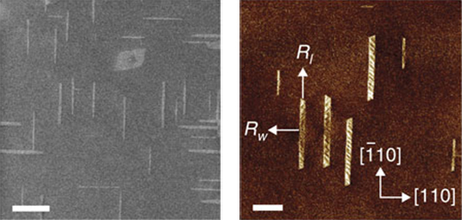
Arnold and his colleagues have now demonstrated a new approach in which they grow graphene directly on a conventional semiconducting wafer made of germanium, using an established industrial process called chemical vapor deposition. Inside a reaction chamber, methane is used to deposit various hydrocarbons on the wafer’s surface, where they react with each other to produce the graphene. The researchers discovered that if they control the temperature and the amount of gas added to the chamber in just the right way, the resulting graphene forms long nanoribbons with the smooth edges that are so desirable for digital applications. As a proof of principle, the group demonstrated working transistors.
Growing smooth-edged nanoribbons directly on a conventional wafer is a very important step. But making computers this way will require vastly more control over the process in order to place billions of identical ribbons in very precise locations, says Jim Hannon, materials science manager for IBM Research. The disadvantage of growing the ribbons, as opposed to starting with a graphene sheet and using lithography to “cut” the sheet into ribbons, is that it’s very hard to control ribbon placement. Hannon says the new approach does offer more control than previous efforts, but much less than what is possible using traditional lithography methods.
Hannon says at this point his group, which is not pursuing nanoribbons, sees more potential for graphene transistors in wireless communication chips. In that application, he explains, making very energy-efficient transistors is not as important, and the lack of a band gap does not present the same problem that it does for digital processors. That means it isn’t necessary to use nanoribbons, much less ones with smooth edges: standard lithography works fine, he says.
Arnold says his group is now focused on understanding the mechanisms underlying the nanoribbons’ growth. He believes it’s reasonable to think the researchers can figure out how to engineer those mechanisms to gain a much greater degree of control over the placement of the nanoribbons as they grow.