How Flake-Handling Trick Will Enable Graphene’s Next Revolution
The ability to stack graphene sheets on top of each other should make possible an entirely new class of devices that exploit previously inaccessible physics, say researchers
In recent months, a new sense of excitement has spread through the graphene research community. These guys are no longer focused on what they can do with single layers of carbon chickenwire. Instead they have a more ambitious plan.
The new goal is to take single layers of high quality graphene and pile them on top of each other to create what physicists call van der Waals heterostructures, layer cakes of carbon crystals each just a single atom thick that promise to behave in entirely new ways. The hope is that this will open the way to undreamt of applications in superconductivity, semiconductor physics and so on.
But there is a problem. Creating layer cakes of crystalline sheets is fraught with difficulty, so research groups around the world are racing to find better ways of doing it.
This story is only available to subscribers.
Don’t settle for half the story.
Get paywall-free access to technology news for the here and now.
Subscribe now
Already a subscriber?
Sign in
Today Xu-Dong Chen and a few buddies at Nankai University in China say they have developed a new and easier way to do it that opens up the possibility of exploring the potential of these devices in much greater detail.
Ideally, physicists would simply grow one layer of graphene on top of another but nobody has worked out how to do this, particularly when they want to orient each layer’s crystal structure in different directions. What’s more, graphene grown in this way is of much lower quality than the stuff they can get by cleaving single layers from a bigger lumps.
This cleaving process creates flakes of high-quality graphene sheets but it also introduces other problems. Nobody has cracked the problem of how to carve these flakes into the required shapes and then to pick them up individually and place them in the required spot.
Hard though it is to credit, the standard technique for gathering high quality graphene is to pick up the flakes using little more than Scotch tape. That sounds better suited to removing fluff from a dinner suit then creating electronic devices of the future.
And indeed it is fraught with problems. The main one is that Scotch tape picks up everything it comes into contact with. So as well as the desired flake, this process also brings a whole load of unwanted flakes too and these can end up contaminating the environment or device into which they are placed.
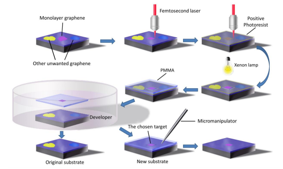
Xu-Dong and co have a more advanced approach that targets specific flakes of graphene, carves them into any desired shape and then picks them up individually so that they can be transferred and placed in a new environment.
The process is relatively straightforward. It begins by identifying the graphene flake to be removed and then carving it into shape with a laser.
The next step is to cover the entire substrate, including all the unwanted graphene flakes, with photoresist and then use the laser to expose the photoresist above the patterned graphene to light. The exposed photoresist is then dissolved to reveal the graphene below.
The final step is to pick up the exposed graphene using the ordinary Scotch tape technique. Since all the unwanted graphene flakes are covered by undissolved photoresist, this only transfers the desired graphene sheet.
Xu-Dong and co have tested their idea by creating a number of graphene patterns and transferring them to other environments. For example, they placed a square sheet of graphene onto a microcavity to create a molecular sieve. They also fabricated graphene ribbons of various widths and thicknesses and transferred them without distortion or fracture. They even use the technique to place graphene structures on top of gold electrodes, an important step in device manufacture.
This new-found ability to selectively transfer sheets of graphene cleanly and accurately is an important enabling step towards creating van der Waals heterostructures. To date, the best attempts have created structures of up to 6 layers but of course physicists want more. This new technique may well give them that.
There are limitations, of course. The new technique requires the hands-on involvement of a researcher at every stage. So it is clearly unsuited to mass production. But that matters little at this stage when physicists are merely attempting to understand the properties and capabilities of this new class of device. The problems of mass production can safely be saved for later.
The promise is huge. Physicists have known for some time now that graphene has extraordinary electronic and mechanical properties. They’ve now spent a decade or so getting to grips with this.
The big question now is what becomes possible when these monolayers are stacked. For example, physicists know that high-temperature superconductivity comes about because of the way that layers of copper oxides are stacked and that the temperature at which superconductivity kicks in is particularly sensitive to the distance between each layer. However the mechanisms involved are unknown.
Graphene is itself a reasonable superconductor so an interesting question is whether its superconducting temperature could be raised by stacking graphene sheets in certain ways or by alternating the sheets with other materials.
It’s this kind of thinking that raises the tantalising prospect that van der Waals heterostructures will be able to exploit previously inaccessible physics.
And that is just the beginning. Physicists are intensely interested in the growing number of other two-dimensional crystals that have been discovered in recent years. These include hexagonal boron nitride, molybdenum disulphide, tungsten diselenide and so on. Just what could be possible with pancakes structures created with these materials is an exciting question to ponder.
And with techniques like this, we may not have long to find out.
Ref: arxiv.org/abs/1308.5514: The Selective Transfer Of Patterned Graphene