A new type of memory chip that a startup company has just begun to test could give future smartphones and other computing devices both a speed and storage boost. The technology, known as crossbar memory, can store data about 40 times as densely as the most compact memory available today. It is also faster and more energy efficient.
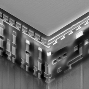
More memory: The memory storage device shown in this electron micrograph image could enable dramatic jumps in the capacity of memory cards and other digital data stores.
The technology’s ability to store a lot of data in a small space could see it replace the flash memory chips that are the basis of memory cards, some hard drives, and the internal storage of mobile devices. Data can be accessed and written to crossbar memory fast enough to see it also possibly compete with DRAM, used as short-term memory, in computing devices. The technology is significantly more energy efficient than both flash and DRAM.
Advertisement
“It will be much denser and faster than flash because it is not based on moving electrons around or on transistors,” says Wei Lu, a professor at the University of Michigan whose research led to the development of crossbar memory. Lu is also a cofounder and chief scientist of the Santa Clara, California-based startup Crossbar, which is commercializing the technology. He notes that initially the company is developing its technology to replace flash storage.
This story is only available to subscribers.
Don’t settle for half the story.
Get paywall-free access to technology news for the here and now.
Demonstration crossbar memory chips are being made by TSMC, the world’s largest contract chip manufacturer. Crossbar says that the current version of the technology can store one terabyte of data (1,000 gigabytes) on a single chip 200 square millimeters, about the size of a postage stamp. By comparison, the densest flash memory chips on the market today store 16 gigabytes on a single chip. The smallest such chip, introduced by Micron in May this year, is 144 square millimeters in area.
Crossbar memory is so called because of the simple nanoscale structure used to store data. Two layers of evenly spaced, rod-like electrodes are stacked on top of one another, with the rods of the top layer oriented at 90 degrees to those of the layer below to form a grid. Bits of data—1s and 0s—are stored at each of the junctions where electrodes from the different layers cross.
That basic crossbar architecture has been used for years as the basis of new ideas in electronics, including for memory (see “Molecular Memory”). However, Lu’s version is different in how it stores data at the junctions, using a simple spacer made from amorphous silicon at each junction rather than a more exotic material.
In Crossbar’s chips, that spacer separates the electrode from the upper layer, made from silver, from that of the lower layer, made from a nonmetallic conductor. Bits are stored by having that spacer flip between being an insulator and a conductor—sometimes allowing current to pass between the upper and lower electrodes, sometimes blocking the current. The spacer can retain its state, and hence a bit, without power.
Data is written by applying a specific control voltage to a particular crossbar junction. Applying a positive voltage causes silver nanoparticles to creep out from the upper rod into the silicon spacer, eventually penetrating far enough to create an electrical path between the upper and lower rods so that current can flow. Applying a negative control voltage can reverse that process. Data is read out from crossbar memory by testing the conductivity of each junction.
In the demonstration chips being produced today, one layer of crossbar memory structures is stacked on top of a layer of conventional silicon CMOS circuitry. That circuitry reads, writes, and erases data from the crossbar memory layers overhead.
Crossbar, which has received $25 million in investment funding from Kleiner Perkins Caufield & Byers, Artiman Ventures, and Northern Light Venture Capital, began working to commercialize Lu’s research in 2010. A crucial part of the development process was adapting the novel technology for mass manufacturing in existing chip factories, says Lu. Experimentation was required to determine how to deposit the novel crossbar structures on top of conventional CMOS circuitry. “You don’t want to contaminate the CMOS layer or to raise the temperature so much that it gets damaged,” says Lu.
Advertisement
Crossbar’s technology is preparing for market at a time when memory manufacturers are struggling to squeeze more data density out of existing methods of making flash memory, says Brian Cronquist, a vice president of Monolithic 3D, a company developing 3-D chip architecture designs. “The ways they used to scale flash memory don’t work anymore.”
Flash memory chips store data as islands of charge on a surface, but those islands cannot be packed any tighter than they are today, making improvements in density practically impossible. That has driven Samsung and Toshiba to work on 3-D flash memory chips, which stack up multiple charge-storing surfaces. Samsung produced working chips ready for mass production earlier this year.
However, Cronquist says, that approach won’t deliver gains for more than a few years, so a new technology will need to take over. Crossbar’s is one possible contender, he says, among others in development.
One of those is HP’s, based on an electrical component known as the memristor, which was predicted to exist in 1971 but first made only in 2008 (see “Memristor Memory Readied for Production”). HP said as recently as last year that it would launch the technology in late 2013, but it has not recently confirmed its plans.