Shortly after David Lam arrived at MIT as a graduate student in nuclear engineering, funding for his focus, nuclear fusion research, began to dry up. Fortunately, plasma, the fourth state of matter, provided an intellectual bridge between nuclear and chemical engineering. Plasma chemistry was then an obscure but promising niche in a department headed by Raymond Baddour, SM ’49, ScD ’51, the MIT professor who became Lam’s lifelong mentor and friend. To Lam, the professor’s book on the application of plasmas to chemical processing was “like a love novel.” Baddour, who later cofounded Amgen, helped Lam catch up on courses he hadn’t taken while studying engineering physics as an undergraduate at the University of Toronto. Upon graduation, he nudged him to leap directly into industry.

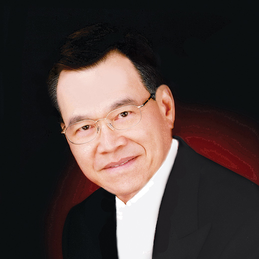
“I was a reluctant chemical engineer and an accidental semiconductor guy, because I had never studied anything to do with semiconductor fabrication,” says Lam. Yet in jobs at Texas Instruments and Hewlett-Packard Labs, he parlayed his graduate work into refining plasma-etching processes for the manufacture of integrated circuits. Living in California in 1980, he launched his own company, Lam Research, to make fully automated plasma-etching equipment that could be used reliably by chip makers in the United States and Japan. Lam Research is now a multibillion-dollar supplier of wafer fabrication equipment and services. In 1984 Lam, who was born in China, became the first Asian-American to take a company public on NASDAQ.
Nearly 30 years later, Lam’s interests and influence have expanded. In 2002, he founded the David Lam Group, which includes Lam Research and nearly a dozen other high-tech ventures that he nurtures through investment and guidance, often as a board member or chair. He has also supported many Silicon Valley professional organizations and served as president of a group now known as the Asia America MultiTechnology Association.
Don’t settle for half the story.
Get paywall-free access to technology news for the here and now.
