Physicists Laser Print Conducting Polymer Circuits
Solvents can cause problems in the manufacture of conducting polymer circuits. The answer is laser printing, say researchers
Conducting polymers are plastics that carry current. This is an emerging technology that is beginning to have a significant impact on areas ranging from photovoltaics and printed circuit boards to batteries and biological sensors.
The advantages of plastic conductors are many. They are cheap, flexible and light. They are also simple to make and to shape into useful circuits. At least in theory.
In practice, most manufacturing techniques have subtle drawbacks that are not easy to overcome. For example, these techniques generally begin with the polymer in liquid form. It is then sprayed, spun or inkjet-coated onto a substrate.
This story is only available to subscribers.
Don’t settle for half the story.
Get paywall-free access to technology news for the here and now.
Subscribe now
Already a subscriber?
Sign in
You’ve read all your free stories.
MIT Technology Review provides an
intelligent and independent filter for the
flood of information about technology.
Subscribe now
Already a subscriber?
Sign in
The problem with liquid polymers is that they require a solvent and this can end up dissolving the layer below, if it is another polymer for example.
Solvents also lead to other problems such as the coffee ring effect in which polymers tend to concentrate at the edge of a droplet as it dries.
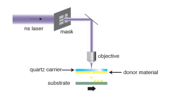
Today, Maria Kandyla at the National Technical University of Athens in Greece and a couple of pals demonstrate a way round this problem that does not rely on liquid polymers. Instead, they use laser ablation to deposit a solid polymer directly onto a substrate, thereby avoiding solvents altogether.
These guys begin by creating a layer of the required conducting polymer on a sheet of glass or quartz. This is called the donor substrate and it is made in the normal way, such as spin coating with liquid and allowing it to dry.
They then place another substrate—the receiving substrate—next to the donor substrate, facing the layer of conducting polymer. However, the two layers do not touch and remain separated by a gap of a few micrometres.
In the final step, Kandyla and co fire a laser through the glass substrate that is focused on the polymer layer. This short burst of energy creates a shock wave that propels a small amount of polymer onto the receiving substrate.
By moving the donor substrate and the receiving substrate, Kandyla and co use this process to deposit 2D patterns of any shape.
And because the polymer transfers as a solid, they avoid all the problems associated with solvents.
Kandyla and co have tested their process by printing photovoltaic circuits of a conducting polymer called P3HT:PCBM onto various substrates.
They’ve also printed biological sensing circuits using a conducting polymer called polyaniline. That’s handy because solvents can interfere with biological measurements and ruin them.
There’s more work ahead of course. One concern is that laser ablation can alter the chemical make-up of polymers. Kandyla and co will have to do more to show that the technique produces high quality circuits in a way that is repeatable at low cost.
And this isn’t the first time that researchers have used laser printing to making conducting circuits from organic materials. LEDs, for example, have already been made in this way.
But the new work extends the range of devices that might benefit from the technique. Expect to hear more about it.
Ref: arxiv.org/abs/1211.3158 : Laser Induced Forward Transfer of Conducting Polymers