The Moore’s Law Moon Shot
It is seemingly a fact of life that every new generation of computing gadget will be significantly more powerful than the one before, but a looming technical roadblock threatens to undermine that.
That’s why the world’s largest chip maker, Intel, announced on Monday that it has invested $4 billion in Dutch company ASML, which makes equipment for manufacturing computer chips.
The two companies are trying to instigate a collaboration involving the world’s largest computing companies—in a kind of silicon moon shot—to ensure that chips keep getting faster by perfecting the tools needed to make smaller features on silicon chips.
“If you have more people to share the risk and contribute, then the prognosis for success as we approach this technological transition goes up,” says Robert Bruck, vice president of Intel’s technology and manufacturing group.
Intel recently launched its first generation of chips with features as small as 22 nanometers. Current methods of making chips will be fine for two generations after—down to 14 nanometers and 11 nanometers. That should keep current methods useful until around 2013, but after that, a new manufacturing technology will be needed. Unfortunately, the best candidate is not only incomplete, but already late.
Significant progress needs to be made in the next few years to keep pace with Moore’s Law, a prediction by an Intel cofounder that has held true since 1975 and underpins consumer and industry expectations that chips will get ever more capable. This law states that the number of transistors that can fit on a silicon chip doubles every two years (the first version of the law, from 1965, said every year), which means that a chip of the same size is more powerful.
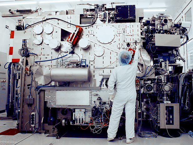
Chip companies chart the progress of Moore’s Law—and set future goals—by comparing the size of the finest details on each generation of chips. The engineers at Intel and other chip companies have always needed to fret over what technical tricks they can come up with to keep that remarkable shrinking on track. Right now, those engineers are staring into something of an abyss.
The technology that promises to keep Moore’s Law going after 2013 is known as extreme ultraviolet (EUV) lithography. It uses light to write a pattern into a chemical layer on top of a silicon wafer, which is then chemically etched into the silicon to make chip components. EUV lithography uses very high energy ultraviolet light rays that are closer to X-rays than visible light. That’s attractive because EUV light has a short wavelength—around 13 nanometers—which allows for making smaller details than the 193-nanometer ultraviolet light used in lithography today. But EUV has proved surprisingly difficult to perfect.
Until 2007, Intel believed that EUV would be used to make the 22-nanometer chips that came out this year, but it opted instead to make fixes that extended the life of lithography based on 193-nanometer light. As recently as 2010, the company hoped to use EUV techniques for the 11-nanometer generation of chips that are still several years away, but once again, technical innovations meant that existing lithography had its retirement canceled.
Delays have also beset EUV. Mostly these have originated with the companies such as ASML and Nikon that develop and sell lithography equipment. One of the biggest challenges has been in making powerful enough sources of EUV light. All types of matter absorb light at these wavelengths, so a source needs to be bright enough to ensure that sufficient light reaches the wafer being worked on. EUV lithography machines are designed to have the beam pass through a vacuum as much as possible, so that air molecules don’t get in the way. Special structures have also been developed to direct and focus the light with minimal absorption, but still, by the time the beam reaches the wafer to be worked on, over 90 percent of the original EUV light has been lost.
ASML’s most complete prototypes can etch components on silicon wafers, but have beams roughly half as strong as what would be needed to mass-produce chips economically. At the same time, the company is trying to make progress on the second generation of EUV lithography technology, which will use complex reconfigurable mirrors to create even finer details on chips. It is also trying to switch to using silicon wafers with just over twice the surface area of those used today, so more chips can be made in a single batch, but this will require new equipment.
Although the Intel deal is formally focused on the next generation of EUV and the switch to larger wafers, the resources it brings should also help ASML address its more immediate problem. “Clearly, there is no next generation if we don’t get this generation working,” says ASML spokesman Ryan Young. “We obviously have to get the first gen finished first.”
In a video statement posted online earlier this week, ASML’s chief financial officer, Peter Wennink, encouraged other chip makers to join the effort to support EUV’s development by signing deals similar to Intel’s, which commits Intel to supporting a large increase in research and development in return for a 25 percent stake in its supplier. Wennink said the whole industry would reap the profits from such agreements. “This is about making sure that the technology that is needed for the next generation chips comes forward faster,” he said. “Ultimately, of course, it will be the consumer that benefits.”
Samsung and Taiwan Semiconductor Manufacturing Company, the two largest chip-making companies after Intel, are the most likely preferred partners, but neither has so far publicly signaled interest. Both Intel and ASML are hoping that these companies and others will put aside their usual competition and pool the funding and expertise needed to get past the roadblock that threatens a coming generation of gadgets.
Keep Reading
Most Popular
Large language models can do jaw-dropping things. But nobody knows exactly why.
And that's a problem. Figuring it out is one of the biggest scientific puzzles of our time and a crucial step towards controlling more powerful future models.
How scientists traced a mysterious covid case back to six toilets
When wastewater surveillance turns into a hunt for a single infected individual, the ethics get tricky.
The problem with plug-in hybrids? Their drivers.
Plug-in hybrids are often sold as a transition to EVs, but new data from Europe shows we’re still underestimating the emissions they produce.
Stay connected
Get the latest updates from
MIT Technology Review
Discover special offers, top stories, upcoming events, and more.