Why metalenses are about to revolutionize chip-making

One of the more amazing new microdevices on the horizon is the metalens. This redesign of the traditional lozenge-shaped lens is a wafer-thin slab of silicon dioxide with a pattern of tiny trenches carved into the surface. The trenches are about the same size as the wavelength of light and influence the passage of photons through the slab, bringing them to a focus.
That turns these slabs into flat lenses. But the real benefit is that they can be carved onto ordinary silicon chips and thus made on the same fabrication lines.
That’s a big step. Until now, lenses have always been made separately and then assembled into optical components. Using metalenses would allow devices such as the cameras in smartphones to be made much more easily and cheaply. Metalenses might even allow entirely new designs of optical components such as optical chips.
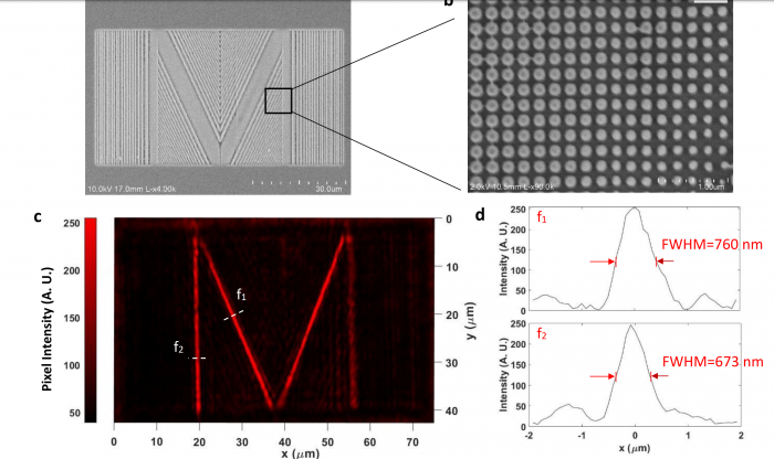
Now Mao Ye and colleagues at the University of Michigan unveil another trick: a set of metalenses that focus light into a specific pattern rather than to a point. That has implications for chip makers who use light to carve specific patterns onto the surface of a silicon slab.
The new technique is straightforward in principle. The idea is that a particular pattern of trenches brings light to a specific focal point. But the researchers then add another pattern with a slightly different focal point that overlaps the first. This creates a focal line.
Adding more patterns with different overlapping focal points increases the complexity of the resulting pattern. In principle, it is possible to create any focal pattern.
Ye and co demonstrate the technique by creating metalenses with a focal pattern in the shape of a U and the shape of an M. This proof-of-principle demonstration shows how lines and curves can be combined to create more complex patterns. “We have proposed and demonstrated a new approach to create metalenses that focus light to an artificially designed pattern instead of a point,” they say.
The technique has a wide range of applications that involve beam shaping: for laser cutting, annealing, and selective crystallization, for example. But it is in chip manufacture where the technique has most promise. “Due to the large energy density that concentrates on the pattern, metalenses of this kind can potentially be applied to next generation nano-lithography with targeted pattern imprinted on the lens,” say Ye and co.
There are improvements still to come. The metalenses designed by Ye and co work at a single wavelength—in this case red light with a wavelength of 685 nanometers.
But other groups have designed metalenses that focus light over a range of wavelengths. Applying the same techniques here should lead to metalenses with focal patterns that work for multiple wavelengths.
That’s interesting work that shows the how metalenses are set to have a significant impact in the coming months and years.
Ref: arxiv.org/abs/1906.10681 : Metalens with Artificial Focus Pattern
Deep Dive
Computing
How ASML took over the chipmaking chessboard
MIT Technology Review sat down with outgoing CTO Martin van den Brink to talk about the company’s rise to dominance and the life and death of Moore’s Law.
How Wi-Fi sensing became usable tech
After a decade of obscurity, the technology is being used to track people’s movements.
Algorithms are everywhere
Three new books warn against turning into the person the algorithm thinks you are.
Stay connected
Get the latest updates from
MIT Technology Review
Discover special offers, top stories, upcoming events, and more.