The next time you place your coffee order, imagine slapping a temperature-sensing sticker onto your to-go cup. Someday, the high-tech stamping that produces such a sticker might also bring us food packaging that displays a digital countdown to warn of spoiling produce, or even a windowpane that shows the day’s forecast, based on measurements of the weather conditions outside.
Engineers at MIT have invented a fast, precise stamping process that may make such electronic surfaces an inexpensive reality. In a paper published in Science Advances, the researchers report having fabricated a stamp made from carbon nanotubes that can print electronic inks onto both rigid and flexible surfaces.
A. John Hart, an associate professor in contemporary technology and mechanical engineering, says the team’s stamping process should be able to print transistors small enough to control individual pixels in high-resolution displays and touch screens. It may also offer a relatively cheap, fast way to manufacture electronic surfaces.
“There is a huge need for printing of electronic devices that are extremely inexpensive but provide simple computations and interactive functions,” Hart says. He adds that the group’s newly developed printing process “is an enabling technology for high-performance, fully printed electronics, including transistors, optically functional surfaces, and ubiquitous sensors.”
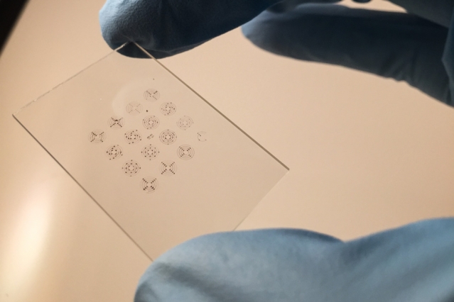
To precisely print electronics, Hart and his team designed “nanoporous” stamps. Spongier than rubber, and about the size of a fingernail, they have patterned features that are much smaller than the width of a human hair.
To create such highly detailed stamps, the team used carbon nanotubes—strong, microscopic sheets of carbon atoms, arranged in cylinders. The researchers used the group’s previously developed techniques to grow the nanotubes on a surface of silicon in carefully controlled patterns, including honeycomb-like hexagons and flower-shaped designs. Then they infused the stamp with a small volume of electronic ink containing semiconducting nanoparticles such as silver, zinc oxide, or quantum dots.
The researchers built a printing machine with a motorized spool, around which flexible substrates can be wound. They fixed each stamp onto a spring-mounted platform to control the force used to press the stamps up onto the substrate as the spool spins over the platform.
Testing revealed that the printed patterns had enough electrical conductivity to serve, for example, as high-performance transparent electrodes. Hart and his team now plan to pursue the possibility of printed electronics.
Keep Reading
Most Popular
Large language models can do jaw-dropping things. But nobody knows exactly why.
And that's a problem. Figuring it out is one of the biggest scientific puzzles of our time and a crucial step towards controlling more powerful future models.
How scientists traced a mysterious covid case back to six toilets
When wastewater surveillance turns into a hunt for a single infected individual, the ethics get tricky.
The problem with plug-in hybrids? Their drivers.
Plug-in hybrids are often sold as a transition to EVs, but new data from Europe shows we’re still underestimating the emissions they produce.
Stay connected
Get the latest updates from
MIT Technology Review
Discover special offers, top stories, upcoming events, and more.