The Nanodevice Aiming to Replace the Field Effect Transistor
The field effect transistor is the workhorse of the consumer electronics industry. Carved into microchips in the billions, these devices beaver away, more or less unnoticed, in practically every home, office, and laboratory in the developed world.
And yet there is a perennial problem with field effect transistors that keeps chip designers awake at night—how to make them ever smaller and thereby keep up the relentless pace of Moore’s Law.
Field effect transistors are already so tiny that making them any smaller leads to a multitude of challenges that are by no means easy to solve. The components of today’s state-of-the-art field effect transistors are just a few nanometers in length—that’s just a few atomic silicon layers thick.
These silicon layers have to be doped with other atoms—just a handful will do the trick in such small components. And therein lies the problem. Even small random variation in the number of dopant atoms in semiconductor components can have a huge effect on the behavior of the transistor. How to control these variations during manufacture is by no means clear. Then there is the physical problem of making a device with three terminals even smaller.
So chip designers would dearly love to have another device they could rely on to build chips that are more densely packed with ever smaller components.
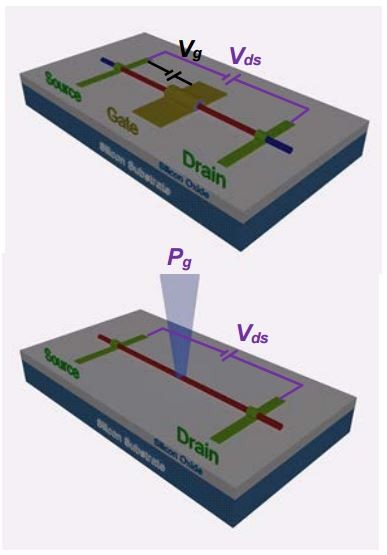
Today, Jason Marmon at University of North Carolina in Charlotte and a few pals unveil just such a device in the form of a light effect transistor. This is essentially a wire that conducts when it is bathed in light and insulates when it is dark. In other words, it is a switch modulated by light. The team says its new device is simpler than a field effect transistor and does not rely on dopant atoms, so it can be made smaller and thereby continue Moore’s law.

First, some background. A field effect transistor is a device with three terminals—a source, a drain, and a gate. The amount of current that flows between the source and drain is determined by the voltage applied to the gate. This switches the current on or off.
A light effect transistor works in an entirely different way. It is simply a nanowire through which current can flow depending on the amount of light hitting it. In other words, it is possible to use light to switch the current on or off.
There is nothing particularly new or special about this photoconductive effect. It occurs when the absorption of light increases the number of electrons and holes in a semiconductor, thereby increasing its conductivity.
However, photoconductive materials have never been suitable as transistors because the effect works only near the surface of the material and does not extend throughout its bulk. So they do not make reliable switches.
But that changes when a photoconductive material is only a few atomic layers thick. In that case, the photoconductive effect occurs throughout the material, making it much more robust as a switch.
Marmon and co’s work consists of characterizing the behavior of semiconducting nanowires made of cadmium and selenium. And they say these wires demonstrate some useful and unique behaviors.
For a start, the wires operate well as switches that by some measures compare well to field effect transistors. For example they allow a million times more current to flow when they are on compared with off when operating at a voltage of about 1.5 V. “[A light effect transistor] can replicate the basic switching function of the modern field effect transistor with competitive (and potentially improved) characteristics,” say Marmon and co.
But they wires also have entirely new capabilities. The device works as an optical amplifier and can also perform basic logic operations by using two or more laser beams rather than one. That’s something a single field effect transistor cannot do.
And the big advantage is that because the photoconductive effect does not require dopant atoms, it is not susceptible to the problems of random variation that plague field effect transistors. Nanowires are also simpler than field effect transistors and so they're potentially cheaper and easier to make.
Of course, there are many hurdles ahead before these devices can be built into integrated chips or even manufactured on an industrial scale. Electronics engineers will want a better understanding of the device’s characteristics in a wider range of conditions, particularly with regard to speed of switching. They’ll also want to know how it fares with modern mass-production manufacturing techniques.
Then there is the question of chip architecture—how do you accurately address a billion or so nanowires with light and how does this affect power consumption?
Nevertheless, light effect transistors offer a range of fascinating possibilities, particularly with regard to optical logic operations. It’ll be interesting to see where the researchers take this next.
Ref: arxiv.org/abs/1601.04748: Light-Effect Transistor (LET) with Multiple Independent Gating Controls for Optical Logic Gates and Optical Amplification
Keep Reading
Most Popular
Large language models can do jaw-dropping things. But nobody knows exactly why.
And that's a problem. Figuring it out is one of the biggest scientific puzzles of our time and a crucial step towards controlling more powerful future models.
The problem with plug-in hybrids? Their drivers.
Plug-in hybrids are often sold as a transition to EVs, but new data from Europe shows we’re still underestimating the emissions they produce.
Google DeepMind’s new generative model makes Super Mario–like games from scratch
Genie learns how to control games by watching hours and hours of video. It could help train next-gen robots too.
How scientists traced a mysterious covid case back to six toilets
When wastewater surveillance turns into a hunt for a single infected individual, the ethics get tricky.
Stay connected
Get the latest updates from
MIT Technology Review
Discover special offers, top stories, upcoming events, and more.