IBM Reports Breakthrough on Carbon Nanotube Transistors
For decades the semiconductor industry has been packing more and more silicon transistors onto each computer chip to keep steadily improving performance, but that process will soon reach its physical limits. Now researchers at IBM say a “major engineering breakthrough” gives reason to be optimistic that a promising alternative to silicon transistors—carbon nanotube transistors—will be ready in time to take silicon’s place.
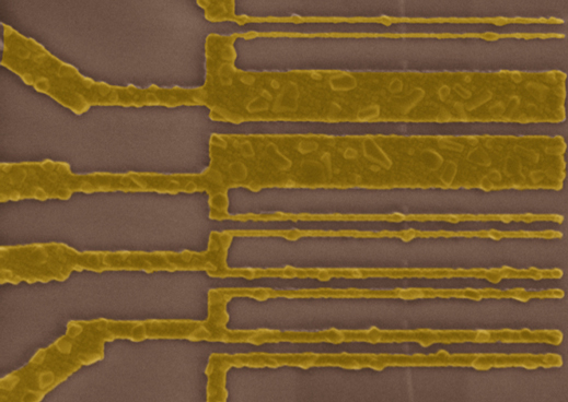
Carbon nanotubes, tiny cylinders made of rolled-up, atom-thick sheets of carbon, have very attractive electrical and thermal properties and theoretically could form the basis of circuits that are much faster and more energy-efficient than today’s silicon ones. But several major manufacturing challenges stand in the way of commercial devices based on nanotube transistors. The IBM researchers say they’ve figured out how to overcome one of them: how to combine nanotubes with the metal contacts that deliver electric current.
Nanotube transistors are a promising alternative because at very small sizes they are more efficient than silicon ones. But early demonstration devices based on nanotubes (see “The First Nanotube Computer”) have had orders of magnitude fewer transistors than are needed for a commercial device, and they’ve used relatively large metal contacts. A commercially viable chip for a high-performing computer would need billions of transistors, and the contacts would have to be a lot smaller. That’s a dilemma, because at this scale the electrical properties of the metal change, and it’s harder to get current into the transistors to switch them. The smaller the contacts get, the worse this problem becomes.
The researchers addressed the issue by changing the interface between a nanotube and the two metal contacts. Instead of depositing them on top of the tube, as in the conventional scheme for building nanotube transistors, they placed them at the ends of the tube and made them react with the carbon to form a different chemical compound. Using this technique, the group demonstrated that contacts less than 10 nanometers long didn’t compromise performance. (Today’s top-of-the-line silicon chips have 14-nanometer features.)
The success of the new method means that the ability to deliver current to carbon nanotube transistors is now independent of the length of the metal contacts, says Wilfried Haensch, who leads IBM Research’s nanotube project. It’s now clear they can make the transistors as small as necessary, he says, and this is a big step toward the company’s goal of having carbon nanotube technology ready by 2020 (see “IBM: Commercial Nanotube Transistors Are Coming Soon”).
Considerable challenges remain, Haensch acknowledges. He says the recent work overcomes only one of the three major hurdles standing in the way of commercially viable carbon nanotube transistors. Another is that nanotubes exist in two forms, metallic and semiconducting, but only the semiconducting ones are useful for transistors. Engineers need to get significantly better at separating metal tubes from semiconducting tubes. The second remaining challenge is developing a reliable, nonlithographic way to place billions of nanotubes exactly where they are needed on a chip.
There has been a lot of progress on the separation problem, says Michael Arnold, a professor of materials science and engineering at the University of Wisconsin, who was not involved in the research. The new result from IBM represents a “fantastic strategy” for addressing the contact problem, he says, though he points out that the researchers have so far only showed it works for one of the two types of transistors needed to perform complementary logic functions. When it comes to aligning nanotubes on the chip, though, a substantial amount of work remains to be done if the technology is to really displace silicon, says Arnold.
Keep Reading
Most Popular
Large language models can do jaw-dropping things. But nobody knows exactly why.
And that's a problem. Figuring it out is one of the biggest scientific puzzles of our time and a crucial step towards controlling more powerful future models.
The problem with plug-in hybrids? Their drivers.
Plug-in hybrids are often sold as a transition to EVs, but new data from Europe shows we’re still underestimating the emissions they produce.
Google DeepMind’s new generative model makes Super Mario–like games from scratch
Genie learns how to control games by watching hours and hours of video. It could help train next-gen robots too.
How scientists traced a mysterious covid case back to six toilets
When wastewater surveillance turns into a hunt for a single infected individual, the ethics get tricky.
Stay connected
Get the latest updates from
MIT Technology Review
Discover special offers, top stories, upcoming events, and more.