Ink-Jet Printing Could Be the Key to Next-Generation OLED Displays
Color-rich, energy-efficient, and flexible displays based on organic light-emitting diodes (OLEDs) could soon be churned out more economically on giant ink-jet printers.
OLED displays are widely expected to eventually supplant LCDs, the most common display today in TVs and computers. OLED displays use less power, have more vibrant colors, and can be made on plastic, making them attractive for flexible and even wearable electronics. The futuristic displays are already appearing in some expensive smartphones, digital cameras, and televisions. But manufacturing challenges have hindered attempts at mass production.
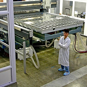
Now the manufacturing equipment maker Kateeva says it has the key to overcoming those challenges. Kateeva’s setup—available as of today to display makers—features a movable platform that precisely positions glass panels or plastic sheets large enough for six 55-inch displays beneath custom print heads. Each head contains hundreds of nozzles tuned to deposit picoliter-scale droplets in exact locations to build up the pixels of a display. The company says the tool can be incorporated fairly easily into existing display production lines.
Kateeva cofounder and president Conor Madigan says the system, based on the same technology in consumer ink-jet printers, eliminates the need for a step in the conventional manufacturing scheme that increases the risk of defects in the displays.
The conventional process takes place in a vacuum chamber. OLED pixels are made by stacking thin films of various organic materials; those layers are deposited by condensing vapors of desired materials onto a surface, usually glass. A fine metal stencil, called a “shadow mask,” sits atop the surface and ensures that the vapors deposit material at extremely precise locations and in uniform patterns.
But relying on the shadow mask is problematic. A large amount of material is wasted because it ends up coating the mask and the walls of the vacuum chamber. And placing and removing the mask has a tendency to introduce defect-causing particles.
Materials that make up OLEDs are very sensitive to contamination—when those materials are exposed to oxygen and moisture during the manufacturing process, it decreases the lifetimes of the resulting devices. Just a few dust particles are enough to ruin a display. And the larger the area of the display being made, the harder it is to control for contamination.
As a result, low manufacturing yields have plagued previous efforts to produce OLED screens large enough for televisions. At this size, the vacuum technique is impractical, argues Madigan. What’s needed, he says, is way to both deposit and pattern OLED material layers with the precision of the shadow mask, but without a shadow mask. This is what the ink-jet printing method promises.
The intricate nature of OLED pixels presents a fundamental challenge, says Vladimir Bulović, an MIT nanotechnologist and Kateeva cofounder. Within the stack of 100 organic molecular layers that make up a display, the glow is provided by only 10—constituting a region just 10 nanometers thick. These layers must be positioned in exactly the right location within the stack to work. Ink-jet printing, he says, offers the accuracy required to achieve this, and to position each pixel precisely in relation to the others in the array.
Researchers have long known that they could use ink-jet printing to make OLED pixels. In fact, it’s been the subject of years of research and development by the printing company Epson and others. But while several companies have tried it, the technology has not yet worked for mass production, says Jennifer Colegrove, president of Touch Display Research. Among other challenges, the lifetimes of printed materials have been too short, she says. But OLED inks have vastly improved in recent years, says Bulović: “The latest material sets are actually extremely stable.”
A potential drawback of switching to ink-jet printing from vacuum deposition is that printing can be a relatively dirty process. Although it reduces particles by eliminating the need for the mask step, “if you don’t design it the right way, it will actually generate a lot of particles,” says Madigan. Reducing the risk of particle contamination has thus been a major focus since Kateeva’s formation in 2008.
Kateeva says it has reduced particle contamination by a factor of up to 10 by devising mechanical systems to reduce ambient turbulence and sweep away dust particles. Further, its system operates in what Kateeva calls the first “production-worthy” all-nitrogen process chamber, an ideal environment for making OLEDs because it prevents exposure to air and moisture.
Bulović says his ink-jet printing company is mimicking the meticulous cleanliness seen in the manufacturing environment of the semiconductor industry, which in its early days struggled to address similar particle-related complications. Such rigor will be crucial to the large-scale manufacturing of OLED displays, he says.
Keep Reading
Most Popular
Large language models can do jaw-dropping things. But nobody knows exactly why.
And that's a problem. Figuring it out is one of the biggest scientific puzzles of our time and a crucial step towards controlling more powerful future models.
How scientists traced a mysterious covid case back to six toilets
When wastewater surveillance turns into a hunt for a single infected individual, the ethics get tricky.
The problem with plug-in hybrids? Their drivers.
Plug-in hybrids are often sold as a transition to EVs, but new data from Europe shows we’re still underestimating the emissions they produce.
Google DeepMind’s new generative model makes Super Mario–like games from scratch
Genie learns how to control games by watching hours and hours of video. It could help train next-gen robots too.
Stay connected
Get the latest updates from
MIT Technology Review
Discover special offers, top stories, upcoming events, and more.