Making Wiring that Doesn’t Trip Up Computer Chips
As chip makers aggressively scale down integrated circuits to provide ever more computing power, much of the focus has been on improving transistors. But performance has also been limited by the copper wiring that shuttles information around the chips.
Today, at the Semicon West conference in San Francisco, semiconductor equipment maker Applied Materials announced a tool that it says solves a part of this problem by making chip wires that have fewer errors. Industry watchers say the new technology may stave off expensive manufacturing problems in the short term.
“Transistors have gotten better as they’ve gotten smaller, and copper wires have gotten worse,” says Robert Geer, professor of nanoscale science at the State University of New York at Albany. As these wires, also called interconnects, get thinner, their electrical resistance increases. The wires that carry signals around state-of-the-art integrated circuits are now the leading sources of power drain, heat buildup, and signal delays.
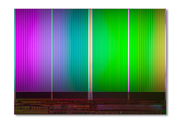
As interconnects have shrunk, they’ve also become trickier to build. It’s this manufacturing problem that Applied Materials’ new machines promise to tackle. Today’s most powerful computer chips are packed with billions of 20-nanometer transistors. Stacked on top of the transistors are tens of insulating layers threaded with copper wiring. At their smallest point, where the wires connect to the transistors, these wires are also about 20 nanometers.
These wires are built one layer at a time by depositing copper into cylindrical holes in the insulating layer. As the copper moves into the tiny but deep holes needed for the next generation of chips, little bubbles tend to form, a catastrophic defect.
Today’s chips contain about 100 kilometers of copper wiring, so the potential for errors is huge. And if one of these wires doesn’t work because of a mistake in one layer—something that’s impossible to detect until the chip is completed and tested—the chip has to be tossed out. Tiny mistakes carry a big price tag: defects at a rate of one per billion lead to a 25 percent drop in yield, says Sree Kesapragada, global product manager for Applied Materials’ metal deposition products.
The company says its new copper-deposition machine, called Endura Amber, can make copper interconnects smaller than 10 nanometers without impacting yield. Like previous machines, it uses a process called ionized physical vapor deposition to coat the chip with a layer of copper. What’s new is that the machine then heats up the chip so that the copper will flow into the hole, reducing the likelihood of defects. Carrying out the deposition and heating steps in the same chamber is not trivial and was something engineers at the company originally considered a “cockamamie idea,” says Kevin Moraes, who manages Applied Materials’ metal deposition products.
This cockamamie idea could help manufacturers use existing chip-making infrastructure for the next generation of chips. But it won’t solve the bigger problem: the fact that smaller copper wires cause major performance problems. “Every incremental advance highlights the fact that you’ve got to work on these big solutions so you can keep up with the huge improvements in computing performance we’re accustomed to,” says Geer.
The solution that would cause the least disruption to chip-making infrastructure would be to find another metal that remains conductive even when made into very thin wires, and which doesn’t heat up as much as copper, says Jonathan Candelaria, director of interconnect sciences at the Semiconductor Research Corporation. Researchers are looking at various alloys, tungsten, or the possibility of returning to aluminum, the interconnect material of choice until about 20 years ago.
For a while, researchers put great hope in new carbon nanomaterials, including graphene. Part of the problem with copper is that electrons scatter off imperfections in the material. Nanotubes and graphene, by contrast, provide smooth sailing for electrons. But researchers are still learning how to work with these materials. So Geer is trying to develop new ways of structuring conventional metals so that, like nanotubes and graphene, they conduct without scattering. Saroj Nayak, professor of physics at Rensselaer Polytechnic Institute in Troy, New York, is also working on tricks to make metal conductors better. He’s developing new insulating materials that put strain on the metal wiring to improve conductivity.
But it’s not clear which of these solutions, if any, will work. Applied Materials would not comment on what it’s prepared for beyond copper. This uncertainty is a big problem, says Candelaria, because it typically takes seven to 10 years to incorporate a new material into semiconductor manufacturing. Meanwhile, copper’s performance problems will become insurmountable in five to 10 years. “We can see this red brick wall of impending doom up ahead,” Candelaria says.
Keep Reading
Most Popular
Large language models can do jaw-dropping things. But nobody knows exactly why.
And that's a problem. Figuring it out is one of the biggest scientific puzzles of our time and a crucial step towards controlling more powerful future models.
The problem with plug-in hybrids? Their drivers.
Plug-in hybrids are often sold as a transition to EVs, but new data from Europe shows we’re still underestimating the emissions they produce.
How scientists traced a mysterious covid case back to six toilets
When wastewater surveillance turns into a hunt for a single infected individual, the ethics get tricky.
Google DeepMind’s new generative model makes Super Mario–like games from scratch
Genie learns how to control games by watching hours and hours of video. It could help train next-gen robots too.
Stay connected
Get the latest updates from
MIT Technology Review
Discover special offers, top stories, upcoming events, and more.