Practical Nanotube Electronics
Carbon nanotubes are a promising material for making display control circuits because they’re more efficient than silicon and can be arrayed on flexible surfaces. Until recently, though, making nanotubes into transistors has been a painstaking process. Now researchers at the University of Southern California have demonstrated large, functional arrays of transistors made using simple methods from batches of carbon nanotubes that are relatively impure.
The pixels in a computer or television screen, whether it’s an LCD or plasma, are each controlled by several transistors. In today’s devices, these transistors are made from silicon. Arrays of these transistors need to be made at high temperatures and in a vacuum, so they’re very expensive, says Chongwu Zhou, an associate professor of electrical engineering at USC and researcher on the nanotube project.
Transistors have also been made from carbon nanotubes, but that, too, presents challenges. “Many people use one nanotube to make a very small, high-performance transistor” for computer chips, says Zhou. But that one-to-one ratio won’t work for displays, in which a large surface must be covered in transistors. “If we use one nanotube for one transistor, the yield will never be high enough” to work for large-scale manufacturing of big screens, he says. Zhou believes his approach will solve this problem by making larger transistors from mats of nanotubes.
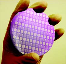
The USC researchers make large arrays of carbon nanotube transistors using solution-processing techniques at room temperature. They start by placing a silicon wafer in a chemical bath to coat its surface with a nanotube-attracting chemical, then rinse off the residue. The treated wafer is then immersed in a solution of semiconducting carbon nanotubes, which are attracted to its surface. The wafer, now coated with a carpet of nanotubes, is rinsed clean again. To make transistors from this tangled mess, the researchers put down metal electrodes at selected locations. The electrodes define where each transistor is and carry electrons into and out of the nanotubes that lie between them. Areas of silicon underlying each device act as the transistors’ gates. So far, they’ve built a prototype device on a four-inch silicon wafer and used it to control a simple organic light-emitting diode display. This work is described online in the journal Nano Letters.
Other researchers have made transistors from nanotube carpets using solution-processing, but these projects started from mixtures of conducting and semiconducting nanotubes, leading to very poor performance. And late last year, researchers at IBM and Northwestern University used highly purified semiconducting nanotubes to make higher-performance transistor arrays in which all the nanotubes line up in nearly straight lines, which improves their electrical properties.
The significance of the USC work is that it shows that arrays made from only 95 percent semiconducting nanotubes that aren’t aligned still have good enough performance for displays, says Zhou.
“This is the first time someone has shown solution-deposited, purified semiconducting tubes for high-quality transistors,” says John Rogers, professor of materials science and engineering at the University of Illinois at Urbana-Champaign. “The accomplishment is in the integration of several promising approaches to demonstrate a full sequence for the fabrication of electronics.”
Now that his group has demonstrated the feasibility of these techniques, Zhou says, it’s working to build a truly integrated organic LED display that is flexible and transparent. Such a display might be rolled up to fit in a pocket, or mounted on a car windshield to display information to the driver. The first step is eliminating the rigid silicon. Because the nanotubes may be laid down at room temperature, the USC researchers can build them on electrically active plastic sheets that can’t tolerate high temperatures. They’re also working to replace the stiff metal electrodes with a coating of indium tin oxide, a commonly used, flexible, transparent electrode material. In their prototype, the organic LED pixels are connected to the transistor array by wires; to integrate them they’ll need to come up with methods for building the LEDs on top of the control circuit.
Zhou says he is talking with display companies about commercializing these methods. Korean display giant LG has demonstrated interest in carbon nanotube electronics, and IBM researchers have been publishing on the topic. However, the only company to come out with a nanotube electronic product so far is the Menlo Park, CA startup Unidym, which makes electrodes from the material.
Researchers in the field have been talking about nanotube displays for years, and the holdup, says Mark Hersam of Northwestern University, has been the lack of a big enough supply of semiconducting carbon nanotubes. In 2006, materials science professor Hersam developed a simple method for purifying nanotubes based on their properties by centrifuging them in a soapy solution. He then founded a company, called NanoIntegris, which has been supplying semiconducting nanotubes to groups including Zhou’s and the research team at IBM. A newly formed company in China and one in Japan are also supplying the semiconducting nanotubes needed for making transistor arrays to control displays.
With this supply in place, says Hersam, it’s only a matter of time before a company comes out with a product, whether it’s made using a method like Zhou’s or some other method. “I’m confident there will be a suite of products in the foreseeable future,” says Hersam. “It’s a matter of going from prototyping to market.”
Keep Reading
Most Popular
Large language models can do jaw-dropping things. But nobody knows exactly why.
And that's a problem. Figuring it out is one of the biggest scientific puzzles of our time and a crucial step towards controlling more powerful future models.
The problem with plug-in hybrids? Their drivers.
Plug-in hybrids are often sold as a transition to EVs, but new data from Europe shows we’re still underestimating the emissions they produce.
Google DeepMind’s new generative model makes Super Mario–like games from scratch
Genie learns how to control games by watching hours and hours of video. It could help train next-gen robots too.
How scientists traced a mysterious covid case back to six toilets
When wastewater surveillance turns into a hunt for a single infected individual, the ethics get tricky.
Stay connected
Get the latest updates from
MIT Technology Review
Discover special offers, top stories, upcoming events, and more.