Printing Electronic Skin
Ali Javey rolls a glass cylinder coated with nanowires over a thin plastic film. With a single motion, he lays down a dense array made up of millions of silicon-germanium nanowires arranged in parallel. Flexible sheets like this one will form the basis for the largest arrays of high-performance nanowire transistors ever made: seven by seven centimeters.
Javey, a professor of electrical engineering and computer science at the University of California, Berkeley, has turned the sheets into pressure sensors that are as sensitive as human skin, which can detect even the tiny force exerted by a fly when it lands on your arm. His “electronic skin” can be made to cover large areas, and it requires very little power. Sheets of the skin could bring a sense of touch to prosthetics, and they could be incorporated into probes used in minimally invasive surgical procedures, providing tactile feedback that would help doctors navigate better.
Javey also plans to use the basic fabrication method to achieve a larger goal: using nanowires to make speedy, flexible low-power electronics for displays. Conventional chips are made of brittle materials, so they can’t be used for applications that require flexibility; flexible organic materials, on the other hand, typically don’t perform well. Many chemists looking for a way to produce high-performance flexible devices have proposed making them from conventional chip materials in the form of nanowires, because nanowires don’t break when arrayed on flexible surfaces. But it’s been difficult to put together arrays of nanowires that perform up to their potential in electronics. Javey’s technique at last provides a way to do this.

PAINTING WITH NANOWIRES
The first step in the process is loading up the roller with nanowires. Javey uses established techniques to grow the nanowires on the surface of the roller, which is simply a glass test tube. Graduate student Toshitake Takahashi coats the outside of the tube with a red liquid containing gold nanoparticles in suspension. Each particle will act as a seed to catalyze the growth of an individual nanowire, whose diameter depends on the particle’s size. Takahashi fits the tube inside a chemical-vapor deposition apparatus. He then closes the chamber, raises the temperature inside to several hundred degrees Celsius, and flows in silane and germane gases, which will provide the ingredients for the silicon-germanium nanowires. The wires sprout up at a rate of about one to five micrometers per minute, reaching their full length in 10 minutes or less.
When the tube is taken out of the machine, nanowires coat its surface like nanoscopic brush bristles, making it appear matte black. Now it’s ready to be used in the printing process, which Javey says originated by accident. “I noticed that rubbing an array of nanowires onto a surface, even by hand, transferred aligned nanowires, as long as you rubbed directionally,” he says. He started transferring the nanowires with a cylindrical roller so that he could print larger arrays at one time.
Javey built the printer, a tiny steel table that supports the printing surface and the roller, in the Berkeley machine shop. The nanowire-coated glass tube fits between two wheels that move along tracks on either side of the device, helping to keep the rolling motion uniform and prevent any wobbling that might misalign the nanowires.

He pushes the roller across a square of polyimide plastic; when the nanowires touch its surface, their tips stick to it. As the roller moves forward, these clinging nanowires are pulled in the same direction and finally detach from the cylinder, all oriented the same way. The process continues until all the nanowires have been transferred to the plastic. To make transistors, Javey uses conventional processes to deposit nickel electrodes and aluminum gates on top of the nanowire arrays.
The uniform orientation of the wires is critical to the performance of nanowire electronics. Researchers have made high-quality transistors from single nanowires, but this requires painstaking techniques that can’t be used for manufacturing. Others have used simpler techniques to make transistors from groups of tangled nanowires without trying to align them. But if the nanowires are in disarray like a pile of pick-up sticks, electrons moving through them take much longer paths and leak out where the wires cross, reducing the current that flows through the transistor and wasting electricity. If the nanowires are all lined up, electrons take a straight path through them and move easily from the tip of one into the next. Javey’s transistors match the performance of single-nanowire transistors but are much easier to produce. “We’re essentially painting wires down,” he says.

THIN-SKINNED
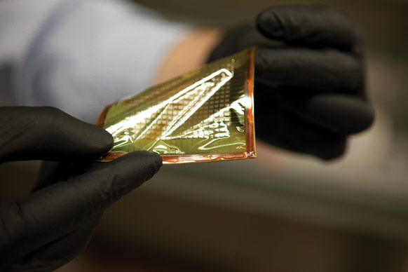
To turn the nanowire array into a pressure sensor, Javey tops it with a sheet of specially treated rubber whose electrical resistance changes when pressure is applied. That causes an abrupt change in the current flowing through the nanowire transistor under that spot; this change can be detected and used to measure the pressure there. The seven-centimeter-square array contains a total of 342 such pressure-sensitive points. The material is so resilient that it can be bent thousands of times without degrading its performance.
In addition to being extremely sensitive, the device requires relatively little power. Pressure sensors have been made with transistors before, but those devices are based on lower-performance organic materials that impose much higher voltage requirements—10 volts, whereas the Berkeley devices can be powered by just two to three volts. Decreasing the voltage, and thus the power consumption, is particularly important for applications such as prosthetics.
Low-power flexible transistor arrays would also be promising for use in displays, says Javey; they could take the place of the heavy, fragile glass-backed arrays of silicon transistors that control the pixels in today’s displays. Future devices could use stacked nanowire arrays, one layer acting as a pressure sensor for a touch screen while another provided electronic controls for display pixels.
Javey’s printing method works with any type of inorganic nanowires, and he’s used it to print active materials for solar cells and light sensors. The ability to generate power, sense light and pressure, and display information might be integrated into lightweight, flexible low-power devices that have yet to be designed. But first, Javey must scale up the technology.
“Right now we’re limited by the size of our tools,” he says. Another problem is that the quality of the nanowire arrays can be inconsistent because the actual printing is done outside a clean room, using “home-built” equipment. “We want to make the process better controlled and get more uniformity with the printing,” says Javey. “If we can improve the process, we’ll transfer it to industry.” Then the technology can be incorporated into commercial products.
“For nanowire devices, this printing approach is the best in town,” says John Rogers, a professor of materials science and engineering at the University of Illinois at Urbana-Champaign. “It offers unprecedented capability at building nanowires into sophisticated devices over areas and at yields that look interesting from a practical perspective.”
Keep Reading
Most Popular
Large language models can do jaw-dropping things. But nobody knows exactly why.
And that's a problem. Figuring it out is one of the biggest scientific puzzles of our time and a crucial step towards controlling more powerful future models.
How scientists traced a mysterious covid case back to six toilets
When wastewater surveillance turns into a hunt for a single infected individual, the ethics get tricky.
The problem with plug-in hybrids? Their drivers.
Plug-in hybrids are often sold as a transition to EVs, but new data from Europe shows we’re still underestimating the emissions they produce.
Google DeepMind’s new generative model makes Super Mario–like games from scratch
Genie learns how to control games by watching hours and hours of video. It could help train next-gen robots too.
Stay connected
Get the latest updates from
MIT Technology Review
Discover special offers, top stories, upcoming events, and more.